 International Defense Security & Technology Your trusted Source for News, Research and Analysis
Related Articles
Remote sensing is the science of acquiring information about the Earth’s surface without actually being in contact with it. This is done by sensing and recording reflected or emitted energy and processing, analyzing, and applying that information. Some examples of remote sensing are special cameras on satellites and airplanes taking images of large areas on the Earth’s surface or making images of temperature changes in the oceans.
Sensors, or instruments, aboard satellites and aircraft use the Sun as a source of illumination or provide their own source of illumination, measuring the energy that is reflected back. Sensors that use natural energy from the Sun are called passive sensors; those that provide their own source of energy are called active sensors. Most passive systems used by remote sensing applications operate in the visible, infrared, thermal infrared, and microwave portions of the electromagnetic spectrum. These sensors measure land and sea surface temperature, vegetation properties, cloud and aerosol properties, and other physical properties. Passive sensors cannot penetrate dense cloud cover, so passive EO satellites can be limited when observing areas like the tropics with dense cloud cover.
Electromagnetic energy, produced by the vibration of charged particles, travels in the form of waves through the atmosphere and the vacuum of space. These waves have different wavelengths (the distance from wave crest to wave crest) and frequencies, These two are inversely related to each other, the shorter the wavelength, the higher the frequency. Some, like radio, microwave, and infrared waves, have a longer wavelength, while others, such as ultraviolet, x-rays, and gamma rays, have a much shorter wavelength.

The infrared (IR) region which covers the wavelength range from approximately 0.7 µm to 100 µm – more than 100 times as wide as the visible portion! The infrared region can be divided into two categories based on their radiation properties – the reflected IR, and the emitted or thermal IR. Radiation in the reflected IR region is used for remote sensing purposes in ways very similar to radiation in the visible portion. The reflected IR covers wavelengths from approximately 0.7 µm to 3.0 µm. The thermal IR region is quite different than the visible and reflected IR portions, as this energy is essentially the radiation that is emitted from the Earth’s surface in the form of heat. The thermal IR covers wavelengths from approximately 3.0 µm to 100 µm.
Infrared waves have longer wavelengths than visible light and can pass through dense regions of gas and dust in space with less scattering and absorption. Thus, infrared energy can also reveal objects in the universe that cannot be seen in visible light using optical telescopes.
Thermal IR radiation can generally be divided into different categories, namely near-wavelength region from 0.8 to 3 μm, mid-wavelength IR (MWIR) region from 3 to 5 μm, and long wavelength IR (LWIR) region from 8 to 12 μm. The MWIR and LWIR regions are most important for free-space communications and astronomy, since the high transparency of the atmosphere at these wavelengths allows transmission without significant losses. The same regions are also widely used for night vision and missile tracking for military applications. IR detection also enables many non-contact, non-destructive inspection methods that are widely utilized in industry, such as automotive and defect detection in electronic circuits
Military requirements
Infrared photodetectors (IRPDs) have become important devices in various applications such as night vision, military missile tracking, medical imaging, industry defect imaging, environmental sensing, and exoplanet exploration. For an IRPD to work, a light-sensitive material capable of absorbing electromagnetic radiation is needed. It converts the absorbed light into a signal that can be collected by a readout device.
Tanks and other military vehicles emit particularly large amounts of heat (mid-infrared radiation) as a result of the engine and equipment operation. For this application the LWIR region is preferred as in the ground combat there are often some smoke or burning vehicles for example. LWIR detectors enable detecting such objects and distinguishing them from the surroundings.
The use of a smart munitions system requires only minimum participation from the user. First, a carrier missile is fired which delivers explosive material to the target area. Next, the main charge with a homing system is separated from the missile and falls freely towards the ground. After the IR sensors are activated and a ground target is detected, the objects identified by means of comparing its parameters with patterns stored in the database. Finally, the proper attack is carried out and the target is effectively neutralized.
Directional Infrared Counter Measures (DIRCM) and Common Infrared Countermeasure (CIRCM) are anti-missile systems. The MWIR region of the IR spectrum is optimal for detecting missiles. The Long-Wave Infrared (LWIR) region is better for degraded environments. A laser installed on the protected object remains off till a threat is detected, so as not to reveal the location of the object. It is the job of an accurate infrared detector to detect the threat. A detector records infrared radiation emitted by the missile, and immediately passes the information on the threat to the missile countermeasure system and to the aircraft/helicopter crew. Next, an active countermeasure system aims its own laser beam at the missile, so that it interprets the beam as the radiation incoming from the target. By means of a suitable modulation of the laser signal, the missile is diverted from the target and neutralized in a safe area.
Stand-off detection is anti-threat solution which could replace soldiers in dangerous areas. This device will be capable of remote control. The long-range device will be designed to search places where an explosion, a gas or terrorist attack may occur. Next, the detection system will notify the operator of the device about possible risks or threats. The present stand-off detection systems are large installations with complicated optical systems, intricate spectroscopes and analyzers. Thanks to the ongoing progress in miniaturization, they may soon become compact systems, easy to transport and convenient to use.
The production of illegal substances creates distinguishable and unique production waste. This chemical waste in gaseous, liquid or solid form can be analysed by infrared system detectors. Large areas can be scannned with the use of drones or aircrafts, and to monitor sewage systems and solid wastes with the use of other measuring devices. In different environments, there are various elements (gas clouds, dust particles, etc.) that may interfere with the measured signal. With this type of interference, detectors operating at high frequencies and with high detection are needed. The development and use of such devices would mean a significant progress in operations conducted in the countries engulfed by conflicts, or in the territories controlled by terrorist organizations.
Infrared guided missiles are an example of the newest generation of weapons which, thanks to their resilience to common and widely used thermal countermeasures, represent a real threat to aircraft and helicopters
For security and defense applications, components carefully adapted to the environmental and mechanical conditions are used in the production of munitions, anti-missile systems or stand-off detection solutions. The detectors’ high sensitivity allows for precise detection of the enemy (smart munitions) or threats (gas attacks, terrorist attacks).
SWaP products: where miniaturization meets performance
Almost every new development, whether embedded, airborne or land-based, carried by military personnel or handheld, shares the same requirement: the need to reduce the size, weight, and amount of available resources used to further contribute to the overall functionality of the system. SWaP stands for Size, Weight and Power. When it comes to military applications, this constant striving for optimization is even more of a priority. Soldiers need increasingly lightweight and compact equipment without compromising on performance. Infrared sensors integrated into military equipment must meet these criteria to improve soldiers’ mobility and efficacy.
Lately, this effort to reduce SWaP has increasingly seemed to be the main deciding factor, leading to some tough compromises on improvements to the performance of the system and multifunctional structures.
MIL standard requirements:
• Strict mechanical tolerances: +/- 0.005 mm
• Strict spectral specifications: wavelength tolerance +/- 0.1 μm
• Short start up / reaction times: 6 s / 8 μs
• Long lifetime: 15 years @ +20 °C
Increased exposures to environmental conditions:
• Low / high temperatures: -50 °C / +80 °C
• Temperature shocks: -40 °C / +50 °C
Increased exposures to mechanical conditions:
• Vibrations: 20 – 500 Hz @ 0.0225 g2 / Hz
• Shocks: up to 20 000 g / 10 ms
• Constant acceleration: up to 40 000 g
IR Detector technology
In order for the absorption process to happen, a semiconductor is used generally. While semiconductor-free methods (such as direct rectification of the electromagnetic radiation, called “rectenna”) have been demonstrated, they have far smaller quantum efficiency compared with the semiconductor-based IRPDs. For different IR regimes or wavelengths, different semiconductor materials with different effective bandgaps are needed for IR detection.
The two main types of IR detectors are thermal detectors and photodetectors. The response time and sensitivity of a photodetector can be higher, but they generally have to be cooled in order to cut thermal noise. The materials in these photodetectors are semiconductors with narrow band gaps.
Mature semiconductor technologies such as mercury cadmium telluride and III–V material-based photodetectors have been dominating the industry.
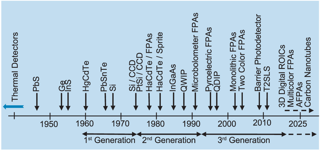
HgCdTe takes the dominant position in infrared (IR) detector technology. This material has triggered the rapid development of the three “detector generations” considered for military and civilian applications. Four generation systems for military and civilian applications can be considered: first generation (scanning systems), second generation (staring systems—electronically scanned), third generation (staring systems with large number of pixels and two-color functionality), and fourth generation (staring systems with very large number of pixels, multi-color functionality, 3D ROIC, and other on-chip functions; e.g., better radiation/pixel coupling, avalanche multiplication in pixels, polarization/phase sensitivity.
However, in the last few decades, significant funding and research has been focused to improve the performance of IRPDs such as lowering the fabrication cost, simplifying the fabrication processes, increasing the production yield, and increasing the operating temperature by making use of advances in nanofabrication and nanotechnology.
IR detector technology combined with the fabrication of epitaxial heterostructure [by molecular beam epitaxy (MBE) and metalorganic chemical vapor deposition (MOCVD)] and photolithographic processes revolutionized the semiconductor industry, thus enabling the design and fabrication of complex focal plane arrays (FPAs).
Further, their development will relate to the implementation of fourth-generation staring systems, which main features are to be: high resolution (pixels > 108 ), multi-band detection, three-dimensional readout integration circuits (3D ROIC), and other integration functions such as polarization/phase sensitivity, better radiation/pixel coupling or avalanche multiplication.
The first three generations of imaging systems primarily rely on planar FPAs. Several approaches to circumvent these limitations, including bonding the detectors to flexible or curved molds, have been proposed. Evolution of fourth generation is inspired by the most famous visual systems, which are the biological eyes. Solution based on the Petzval-matched curvature allows the reduction of field curvature aberration.
In addition, it combines such advantages as simplified lens system, electronic eye systems and wide field-of-view (FOV). The colloidal quantum dot (CQD) and 2D layered material photodetectors fabricated on flexible substrates exhibit the potential to circumvent technical challenges in the development of the fourth generation IR systems.
The photodetector performance (detectivity bandwidth product) can be enhanced by two methods. First method is based on engineering the electronic properties of the absorbing material for improved figures of merits such as detectivity and quantum efficiency. The second method is based on increasing the coupling of light to the electronic states of the absorbing material.
In the last two decades, several new concepts for improving the performance of infrared detectors have been proposed. These new concepts particularly address the drive towards the so-called high operating temperature focal plane arrays (FPAs), aiming to increase detector operating temperatures, and as a consequence reduce the cost of infrared systems.
The need for cooling considerably limits more widespread use of IR technology. There are significant attempts to decrease system size, weight, and power consumption (SWaP) to limit IR system’s cost and to increase the operating temperature. The invention of microbolometer array was a milestone step in development of IR cameras operating at
300 K. However, microbolometers belong to the class of thermal detectors with limited response time—typically in millisecond range and could not be used in the multiband applications. To omit this limitation, further efforts are directed to increase operating temperature of photon detectors.
Currently nanostructures such as graphene, 2D materials, quantum well (QW), quantum dot (QD), SLS and colloid quantum dot (CQD) have shown to dramatically improve the electronic properties of IRPDs. In particular, Graphene based photodetectors are capable of detecting the entire spectrum, from infrared to visible to ultraviolet and in future would lead to ultrasensitive detectors and that too at room temperature.
In addition to photoresistors and photodiodes, three other types of IR detectors can operate at near 300 K: magnetic concentration detectors, photoelectromagnetic (or PEM) detectors and Dember effect detectors.
New technology allows cameras to capture colors
In Nov 2020, researchers from Tel Aviv University developed technology that will allow cameras to recognize colors that the human eye and even ordinary cameras are unable to perceive. The technology makes it possible to image gases and substances such as hydrogen, carbon and sodium, each of which has a unique color in the infrared spectrum, as well as biological compounds that are found in nature but are ‘invisible’ to the naked eye or ordinary cameras.
But in their study, TAU researchers were able to develop cheap and efficient technology that could mount on a standard camera and allows, for the first time, the conversion of photons of light from the entire mid-infrared region to the visible region, at frequencies that the human eye and the standard camera can pick up. Existing infrared detection technologies are expensive and mostly unable to render those “colors.” In medical imaging, experiments have been performed in which infrared images are converted into visible light to identify the cancer cells by the molecules. To date, this conversion required very sophisticated and expensive cameras, which were not necessarily accessible for general use.
“We humans can see between red and blue. If we could see in the infrared realm, we would see that elements like hydrogen, carbon and sodium have a unique color,” explains Prof. Suchowski. “So an environmental monitoring satellite could ‘see’ a pollutant being emitted from a plant, or a spy satellite would see where explosives or uranium are being hidden. In addition, since every object emits heat in the infrared, all this information could be seen even at night.”
II–VI-based IRPD
The II–VI material system, such as HgCdTe, is one of the most important semiconductor alloy systems and the most commonly used material for IR detectors in the spectral range between 1 and 25 μm. The HgCdTe ternary alloy is an ideal IR material system due to these key features: composition-dependent tailorable energy bandgap, high optical absorption coefficient, high quantum efficiency and favorable inherent recombination mechanisms leading to long carrier lifetimes and high operating temperatures. The attributes of HgCdTe translate to flexibility and the capability to produce SWIR, MWIR, and LWIR detectors.
University of Chicago use Quantum Dots to enable cheaper infrared cameras
A new breakthrough by scientists with the University of Chicago, however, may one day lead to much more cost-effective infrared cameras—which in turn could enable infrared cameras for common consumer electronics like phones, as well as sensors to help autonomous cars see their surroundings more accurately. “Traditional methods to make infrared cameras are very expensive, both in materials and time, but this method is much faster and offers excellent performance,” said postdoctoral researcher Xin Tang, the first author on a study which appeared Feb. 25 in Nature Photonics.
“That’s why we’re so excited about the potential commercial impact,” said co-author Philippe Guyot-Sionnest, a professor of physics and chemistry. Today’s infrared cameras are made by successively laying down multiple layers of semiconductors—a tricky and error-prone process that makes them too expensive to go into most consumer electronics.
Guyot-Sionnest’s lab instead turned to quantum dots—tiny nanoparticles just a few nanometers in size. (One nanometer is how much your fingernails grow per second.) At that scale they have odd properties that change depending on their size, which scientists can control by tuning the particle to the right size. In this case, quantum dots can be tuned to pick up wavelengths of infrared light.
This ‘tunability’ is important for cameras, because they need to pick up different parts of the infrared spectrum. “Collecting multiple wavelengths within the infrared gives you more spectral information—it’s like adding color to black-and-white TV,” Tang explained. “Short-wave gives you textural and chemical composition information; mid-wave gives you temperature.”They tweaked the quantum dots so that they had a formula to detect short-wave infrared and one for mid-wave infrared. Then they laid both together on top of a silicon wafer.
The resulting camera performs extremely well and is much easier to produce. “It’s a very simple process,” Tang said. “You take a beaker, inject a solution, inject a second solution, wait five to 10 minutes, and you have a new solution that can be easily fabricated into a functional device.” There are many potential uses for inexpensive infrared cameras, the scientists said, including autonomous vehicles, which rely on sensors to scan the road and surroundings. Infrared can detect heat signatures from living beings and see through fog or haze, so car engineers would love to include them, but the cost is prohibitive.
They would come in handy for scientists, too. “If I wanted to buy an infrared detector for my laboratory today, it would cost me $25,000 or more,” Guyot-Sionnest said. “But they would be very useful in many disciplines. For example, proteins give off signals in infrared, which a biologist would love to easily track.”
QW-based IRPD
A Quantum Well Infrared Photodetector (QWIP) is an infrared photodetector, which uses electronic intersubband transitions in quantum wells to absorb photons. The basic elements of a QWIP are quantum wells, which are separated by barriers. Among the different types of QWIPs, GaAs/AlGaAs QW detectors are the most mature due to the almost perfect natural lattice match between GaAs and AlGaAs . GaAs/AlGaAs QW devices have many advantages, including their ability to be used with standard GaAs based manufacturing techniques and processing technologies, highly uniform and well-controlled molecular beam epitaxy growth on six-inch GaAs wafers, high yield and thus low cost, more thermal stability, and extrinsic radiation hardness.
New emerging nanomaterials for detection
Graphene was the first 2D material which attracted the attention of many scientists due to its appealing features for nanophotonic applications originating from its zerobandgap nature. With linear dispersion near the Dirac point and various forms of light-matter interaction, graphene offers a high optical responsivity in a broad spectral range. However, graphene has low absorption as an IRPD, which is due to its short carrier lifetime and its zero-bandgap nature. This gives rise to interest in another family of 2D materials – the single-layer TMDCs , such as molybdenum disulfide (MoS2) and tungsten diselenide (WSe2). Unlike graphene, the TMDC family has indirect-to-direct bandgap transitions that occur when the material thickness decreases from multilayer to monolayer. Moreover, TMDCs can easily be incorporated into a wide range of heterostructures with atomic-level control to achieve a higher performance IRPD.
Graphene based IR detectors
Researchers from MIT, Harvard University and Army Research Laboratory have integrated graphene based photo thermo-electric detectors with micro machined silicon nitride membranes, thereby enabling detection as well as stand-off imaging of an incoherent blackbody target (300–500 K) such as normal person at room temperature without cryogenic cooling.
DARPA has awarded a $1.3 million grant to a team led by University of Central Florida researcher Debashis Chanda to fund the development of a next-generation IR detector that could be used in night vision, meteorology and space exploration.
Navy engineer employs metamaterial to enhance night vision for ground forces
A Navy engineer has invented a groundbreaking method to improve night vision devices without adding weight or more batteries. Dr. Ben Conley, an electro-optics engineer at the Naval Surface Warfare Center-Crane Division, has developed a special metamaterial to bring full-spectrum infrared to warfighters. On August 28, 2018 the Navy was granted a U.S. patent on Conley’s technology.
“Our ground forces will be able to see much more, with better clarity, in all environments including caves and tunnels,” Conley told TechLink. “Enemy forces hiding in the bushes? No problem, we’ll see their body heat.” Instead of treating infrared light as a particle as most physicists do, Conley, a Marine combat vet, treats it as a wave. Using tiny metal structures (you’d need 25 of them to equal the width of a human hair), Conley built an infrared antenna that can see the waves. Conley’s metamaterial antenna will expand the sensed spectrum, adding short and mid-wavelength infrared.
The sights and goggles, then and now, intensify visible light and just a bit of near-infrared radiation. This isn’t a new concept, but other “fusion” devices combining near-infrared and infrared together are bigger and require additional battery power that increases system weight. That’s a no-no in the world of ground combat where lighter is always better. Conley’s new infrared image intensifier, or “I-cubed,” as he calls it, will add no weight and require no additional battery power.
In coordination with the Technology Transfer Office at NSWC-Crane, TechLink, the Department of Defense’s national partnership intermediary for technology transfer, is marketing the technology to companies for night vision devices or other applications like machine vision, thermal imagers, security systems, and self-driving cars.
Ultrathin TLA Materials Could Broaden IR Applications
High-quality detectors cost approximately $100,000, some require cooling to -200°C. Now, research spearheaded by researchers at the University of Sydney has demonstrated a dramatic increase in the absorption efficiency of light in a layer of semiconductor that is only a few hundred atoms thick – to almost 99 percent light absorption from the current inefficient 7.7 percent.
Ultrathin gratings composed of common materials were shown to increase the absorption efficiency of light to almost 99 percent when thin grooves were etched into the film, directing the light sideways. The semiconductor materials are compatible with optoelectronic applications such as photodetectors and optical modulators, and could make IR technology less expensive and more accessible.
Researcher Björn Sturmberg said the findings did not rely on a particular material but could be applied to many naturally occurring weak absorbers. “There are many applications that could greatly benefit from perfectly absorbing ultrathin films, ranging from defense and autonomous farming robots to medical tools and consumer electronics,” Sturmberg said.
Nanostructure-based AR coating and light trapping effect
A possible way to increase the absorption probability, while at the same time keeping the detector optical thickness constant, is to ensure a longer path of light through the detector and to maximize the incident light on the structure. The idea is to maximize the incident light and trap the light that has already entered the active region and keep it as long as possible. The beam could be returned into the detector from its surface, immediately before leaving the structure. The incident optical flux into an optical element can be maximized by decreasing reflection from the incident surface.
One the most commonly used light-trapping structures in IRPDs is the resonant cavity structure. The absorption within the detector can be significantly increased by placing the active area into a resonant cavity between resonator mirrors (usually consisting of a highly reflective mirror and a distributed Bragg mirror). A field of research that is currently exponentially growing is light-matter interaction structures such as plasmonic and nanoantenna.
New Photodetector Enables NASA’s Thermal Imager
A compact thermal camera named the Compact Thermal Imager, or CTI, has been developed by NASA using photodetector technology known as strained-layer superlattice, or SLS, which will be demonstrated on an upcoming robotic servicing demonstration mission.
The SLS assembly is a large-format detector, measuring nearly 16 in. long and 6 in. tall. It consumes little power, operates at liquid-nitrogen temperatures, is easily fabricated in a high-technology environment, and is inexpensive almost to the point of being disposable, according to engineer Murzy Jhabvala.
The detector technology is also quickly and easily customized for different applications, Jhabvala said. The Goddard Detector Development Laboratory, for example, recently fabricated a 1024- x 1024-pixel SLS array and plans to increase its size to 2048 x 2048 pixels in the very near future.
Jhabvala collaborated with his industry partner, the New Hampshire-based QmagiQ, to develop the SLS detector assembly. The SLS is based on the quantum well infrared photodetector, or QWIP, technology that Jhabvala and his government and industry collaborators spent more than two decades refining.
Compared with its predecessor, the SLS detector is 10 times more sensitive and operates over a broader IR spectral range and at substantially warmer temperatures — 70 K for the SLS array compared with 42 K for the QWIP array. Because the SLS array can operate at warmer temperatures, its cooling system can be smaller, and so it consumes less power.
During NASA’s next Robotic Refueling Mission 3, the CTI will image and measure fires, ice sheets, glaciers, and snow surface temperatures on Earth’s surface. It will also measure the transfer of water from soil and plants into the atmosphere.
The CTI and its SLS detectors will employ a hybrid computing system that will control the instrument and process the images and video that it takes while in orbit.
The demonstration’s goal, Jhabvala said, is to raise SLS’s technology-readiness level to nine — meaning that it has flown in space and has demonstrated that it operates well under the extreme environmental conditions found in space
This is a very important technology milestone,” Jhabvala said. “We needed this mission. When we demonstrate our detector array, multiple copies can be made, assembled, and aligned into focal plane arrays that would allow us to image large swaths of Earth’s surface from space in the future.”
DARPA’s Low Cost Thermal Imager program
DARPA’s “low cost thermal imager” program is aimed at refining, manufacturing for infrared sensors to make them small enough to embed in smartphones, rifle sights or eyeglasses and affordable enough to purchase for every soldier.
DARPA and its industry partners were able to shrink pixel size to 12 and 10 microns. “As the pixel size gets smaller, it allows us to make the sensors much smaller and it allows us to increase the resolution without making the sensor larger,” Dhar said. They also developed new optical materials that can be stamped on a wafer in the same way cell phone cameras are manufactured.
Infrared Detector Market
The global military infrared imaging systems market grew by 5% in 2020, as new detector technologies were incorporated into systems. Thru 2025, the military infrared imaging systems market is expected to grow at a compound annual rate of 7%.
The overall Infrared detector market is expected to grow from USD 446 million in 2021 to USD 619 million by 2026, at a CAGR of 6.8%. An infrared detector is an electronic device used to detect infrared radiation by sensing the surrounding environment. Infrared detectors can sense infrared spectrum ranging from wavelengths 0.7 ìm to 1 ìm. Various types of infrared detectors are available in the market, e.g., mercury cadmium telluride (MCT/HgCdTe), indium gallium arsenide (InGaAs), microbolometer, pyroelectric, and thermopile infrared detectors. They find applications in people & motion sensing, temperature measurement, security & surveillance, gas & fire detection, and spectroscopy & biomedical imaging in the industrial and nonindustrial verticals.
The infrared thermal imaging detector chip is the core of the infrared industry, and its performance directly determines the resolution and sensitivity of infrared thermal imaging equipment.
Pyroelectric segment to hold the largest share of the Infrared detector market, by type, in 2021
This segment is expected to hold its dominating position during the forecast period. People and motion sensing is the key application area of pyroelectric infrared detectors. Every object or substance emits some radiant energy, known as infrared radiation, which can be detected by infrared detectors. Pyroelectric infrared detectors use passive infrared (PIR) technology, which can detect the amount of infrared radiation radiated from an object/substance. These detectors can also identify the changes in the amount of radiation, which depends on the change in temperature of the object. Passive infrared detector devices do not generate or radiate any energy for detection. PIR-based motion detectors are used to sense the movement of people, animals, objects, and substances. Excelitas Technologies (US), Nippon Ceramic (Japan), and Murata Manufacturing (Japan) are some of the key manufacturers of pyroelectric infrared detectors.
The market for people and motion sensing application to grow at the highest CAGR during the forecast period
Infrared detectors are used in people and motion sensing applications for detecting the movement of an object or human beings. People and motion sensing devices are widely used in retail stores, stadiums, shopping malls, and museums for counting the number of people entering and leaving the particular space and observing their movements. Besides, these detectors are also increasingly being used in commercial and residential infrastructure for building automation and increasing safety. For instance, infrared sensors are being used in smart lighting systems for presence detection, which enables the lights to be switched on and off automatically after detecting the presence of any living being. Another example of the application of infrared detectors in buildings is their use in security systems. Security systems use infrared detectors or sensors to identify thieves and robbers. Infrared detectors are fixed on the side of windows. These detectors raise the alarm when a person is detected at the window. A pulse is transmitted by the infrared detector, which is transferred to the alarm system to raise the alert. Passive infrared sensors (PIR), also known as pyroelectric sensors, are commonly used for people and motion sensing application. Automotive is another emerging segment where infrared detectors are used for people detection.
North America to hold the largest share of Infrared detector market by 2021
The infrared detector market in North America has been further classified into the US, Canada, and Mexico. The regional market growth is dominated by major companies such as Excelitas Technologies (US), Texas Instruments (US), Honeywell International (US), and FLIR Systems (US). These companies are striving to expand their presence in emerging markets such as APAC. Prominent companies in the infrared detector market are also acquiring, collaborating, and partnering with companies from various industries such as automotive and military & defense to broaden their product portfolio and expand their presence. For instance, in October 2019, FLIR Systems (US) partnered with Veoneer (US), a tier-one automotive supplier, to provide thermal sensing technology for use in Veoneer’s self-driving cars.
The major global thermal imaging camera market players such as Bullard, Cox, Fluke Corporation, InfraTec GmbH Infrarotsensorik und Messtechnik, Opgal, SATIR, Seek Thermal, Synectics Plc, Teledyne FLIR LLC, and Thermoteknix Systems Ltd.
References and Resources also include:
https://www.degruyter.com/downloadpdf/j/nanoph.2018.7.issue-1/nanoph-2017-0061/nanoph-2017-0061.pdf
https://www.photonics.com/Articles/New_Photodetector_Enables_NASAs_Thermal_Imager/a63749
https://www.eurekalert.org/pub_releases/2018-09/t-ned091918.php
https://phys.org/news/2019-03-breakthrough-enable-cheaper-infrared-cameras.html
https://www.marketsandmarkets.com/PressReleases/ir-detector.asp