International Defense Security & Technology Your trusted Source for News, Research and Analysis
Related Articles
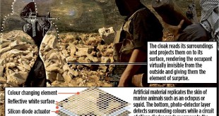
While the conventional electronics like computers and smartphones is built around silicon integrating billions of transistors and is manufactured using complex, costly and wasteful processes in multi-billion dollar foundries , The printed and flexible electronics aim to replace this by “organic” semiconductors which are long chains of thousands of repeating molecules (a plastic), made with materials based on carbon. Organic semiconductors can be made to be soluble, and can be turned into an ink. This means it’s possible to print electronic circuits, with the potential to manufacture components as fast as printing newspapers. A printer would do this by applying different inks onto the film. As the inks dried, they would turn into wires, transistors, capacitors, LEDs and all the other things needed to make displays and circuits.
Printed electronics is a set of printing methods used to create electrical devices on various substrates. Electrically functional electronic or optical inks are deposited on various substrates (mainly plastics and fabrics), creating active or passive devices, such as thin film transistors, capacitors, coils and resistors.
Printed electronics is expected to facilitate widespread, very low-cost, low-performance electronics for applications such as flexible displays, smart labels, decorative and animated posters, and active clothing that do not require high performance.
Both organic and inorganic materials are used for printed electronics. Ink materials must be available in liquid form, for solution, dispersion or suspension. They must function as conductors, semiconductors, dielectrics, or insulators. Some tried and tested materials include organic, conductive polymers and nanoparticles made of conductive oxides (TCOs). Common printing equipment suitable for defining patterns on material, such as screen printing, flexography, gravure, offset lithography, and inkjet are used.
Printed and flexible electronics have thus far failed to achieve widespread adoption due to significant unresolved technical challenges. Major gaps exist between expectations and performance of printed electronics in the areas of logic, memory, analog circuitry, power, and light generation.
However Printed electronics have evolved substantially from the early implementations of basic conductive copper or silver traces printed on hard (and later flexible) substrates to which conventional electronic components were attached. Now, thanks to advances in materials science, printed electronics incorporates a wide variety of capabilities, from roll-to-roll memories to printable thin film transistor (TFT) logic and even wireless communications.
The global printed electronics market size was almost $30 billion in 2017 and a growth potential to over $70 billion in ten years. The surging demand for the flexible electronics at low manufacturing costs and the need for eco-friendly technologies is paving the way for increased adoption of the technology. Additionally, the increasing penetration of IoT worldwide is proving to be a prime factor in pulling the printed electronics market over the forecast period. The continuously growing demand for IoT in the telecommunication industry for enhancing the network and optimizing the performance along with operations is expected to propel the application of technology over the forecast period.
Key Printing Techniques
The difference between normal printing and printed electronics is that in printed electronics, functional material is used as ink that exhibits functionalities of insulator, conductor, and semiconductor materials, which are essential for the electronic devices. In most of the fabrication of electronic devices, these materials are sprayed over the substrate with the help of printing technology as low as few nanometers thick (thin film) and few micrometers width (pattern). The combination of thin films and patterns can make any electronic device to be used in the electronic circuits.
Although the process seems simple, but the limitations posed by the various parameters such as uniformly dispersed and stable colloidal solutions, substrate treatments, and above all, optimized printing recipes make the printing process much more challenging. As compared to conventional electronic manufacturing, printing technologies are revolutionizing the incredible field of flexible/bendable electronics by providing cost-effective routes for processing diverse electronic materials on nonplanar substrates at compatible temperatures. Simplified processing steps, reduced materials’ wastage, low-fabrication costs, and simple patterning techniques make printing technologies very attractive when compared to standard microfabrication in clean room processes.
Spin Coating / Doctor Blading
Spin coating, often referred to as doctor blading, is one of the most commercially-available methods of printing electronic elements onto functional substrates. It is a diverse technology in its own right, but each subset of spin coating tends to follow the same basic theory: A nanoparticle dispersion is deposited onto a substrate that is mounted on / adhered to a rotatable platform. Once the dispersion has fully covered the substrate, the platform rotates at high speed, shedding most of the ink from the surface. The remaining material is allowed to dry, leaving a uniform thin film of just nanometres (nm) or micrometers (μm) in thickness.
Slot Die Coating
Slot die coating is a unique method of generating printed electronics using pre-metered deposition of nanoparticle inks. Rather than rely on centrifugal force to disperse a coating across a substrate, a slot-die machine uses a printing head integrated into a metering system to continuously deposit solutions at pre-defined flow rates. Depending on the size and scale of operations, the equipment may also involve a CNC head-positioning system and a substrate positioning component.
Larger-scale producers of printed electronics have found significant success using slot-die machines in roll-to-roll processing, with rapid workflows and high throughput.
Ink Jet Printing
The term ink jet printing is the most familiar method of generating printed electronics, drawing on classical computer printing techniques. An ink jet printer uses a series of nozzles to deposit nanosized coatings onto a substrate in a series of droplets, significantly reducing wastage associated with excessive deposition.
Screen Printing
One final printing technique worth exploring is screen printing; a unique method whereby nanoparticle inks are forced through an extremely fine screen with a pre-rendered stencil. This stencil forms the basis of the conductive pattern underlying the many electronic functionalities of the end-product.
New hybrid inks permit printed, flexible electronics without sintering
Research scientists at INM — Leibniz-Institute for New Materials have now combined the benefits of organic and inorganic electronic materials in a new type of hybrid inks. This allows electronic circuits to be applied to paper directly from a pen, for example.
To create their hybrid inks, the research scientists coated nanoparticles made of metals with organic, conductive polymers and suspended them in mixtures of water and alcohol. These suspensions can be applied directly on paper or foil using a pen and they dry without any further processing to form electrical circuits.
Scientists develop a new method to revolutionize graphene printed electronics
The development of printed conductive inks for electronic applications has grown rapidly, widening applications in transistors, sensors, antennas RFID tags and wearable electronics. Current conductive inks traditionally use metal nanoparticles for their high electrical conductivity. However, these materials can be expensive or easily oxidised, making them far from ideal for low cost IoT applications.
The team have found that using a material called dihydrolevogucosenone known as Cyrene is not only non-toxic but is environmentally- friendly and sustainable but can also provide higher concentrations and conductivity of graphene ink. Professor Zhiurn Hu said: “This work demonstrates that printed graphene technology can be low cost, sustainable, and environmentally friendly for ubiquitous wireless connectivity in IoT era as well as provide RF energy harvesting for low power electronics”.
Professor Sir Kostya Novoselov said: “Graphene is swiftly moving from research to application domain. Development of production methods relevant to the end-user in terms of their flexibility, cost and compatibility with existing technologies are extremely important. This work will ensure that implementation of graphene into day-to-day products and technologies will be even faster”. Kewen Pan, the lead author on the paper said: “This perhaps is a significant step towards commercialisation of printed graphene technology. I believe it would be an evolution in printed electronics industry because the material is such low cost, stable and environmental friendly”.
The National Physical Laboratory (NPL), who were involved in measurements for this work, have partnered with the National Graphene Institute at The University of Manchester to provide a materials characterisation service to provide the missing link for the industrialisation of graphene and 2-D materials. They have also published a joint NPL and NGI a good practice guide which aims to tackle the ambiguity surrounding how to measure graphene’s characteristics.
Professor Ling Hao said: “Materials characterisation is crucial to be able to ensure performance reproducibility and scale up for commercial applications of graphene and 2-D materials. The results of this collaboration between the University and NPL is mutually beneficial, as well as providing measurement training for Ph.D. students in a metrology institute environment.” Graphene has the potential to create the next generation of electronics currently limited to science fiction: faster transistors, semiconductors, bendable phones and flexible wearable electronics
New graphene based inks for high-speed manufacturing of printed electronics
Researchers at the University of Cambridge in collaboration with Cambridge-based technology company Novalia, have developed a low-cost, high-speed method for printing graphene inks using a conventional roll-to-roll printing process, like that used to print newspapers and crisp packets.
The method allows graphene and other electrically conducting materials to be added to conventional water-based inks and printed using typical commercial equipment, the first time that graphene has been used for printing on a large-scale commercial printing press at high speed. “This method will allow us to put electronic systems into entirely unexpected shapes,” said Chris Jones of Novalia. “It’s an incredibly flexible enabling technology.
Currently, printed conductive patterns use a combination of poorly conducting carbon with other materials, most commonly silver, which is expensive. Silver-based inks cost £1000 or more per kilogram, whereas this new graphene ink formulation would be 25 times cheaper. Additionally, silver is not recyclable, while graphene and other carbon materials can easily be recycled. The new method uses cheap, non-toxic and environmentally friendly solvents that can be dried quickly at room temperature, reducing energy costs for ink curing. Once dry, the ‘electric ink’ is also waterproof and adheres to its substrate extremely well.
Printing Active devices
Printed active devices today have very limited performance. A significant limitation of the printing processes and materials available today is the inability to print active electronic devices entirely. While printing can produce reliable and versatile sensing probes (either singly or in arrays), these do not offer much without a suitably formatted processing capability to read the sensors, condition the data, communicate it, and perhaps display it.
“There are at least two options here. First, a collaboration including Xerox Palo Alto Research Center (PARC) and Thin Film Electronics ASA resulted in printable TFT transistors. Second, a hybrid printed manufacturing process called printed dopant polysilicon (PDPS) has been developed to address RF and other applications that require high-performance transistors, which we’ll explore further,” writes Matthew Bright, Thin Film Electronics ASA
“The PDPS process, which enables NFC barcode and sensor-based NFC smart label products, enables the design of printable, high-frequency RF circuits for printed systems connected to smartphones using NFC. The addition of NFC capability has opened up a new spectrum of smartphone-centric applications, some of which are only just starting to take shape.”
One recently commercialized core building block in printed electronics is printed memory. The printed memory works on the principle that when a voltage is applied to a ferroelectric polymer material the dipoles within the polymer layer align in one of two directions, depending on whether the voltage is applied to the top or bottom electrode. When voltage is removed, the material remains in the same state and can be read as a one or a zero, making it equivalent to a non-volatile memory (NVM) cell, but at lower cost and available in a thin, flexible self-adhesive label.
Printed electronics breakthrough could lead to flexible electronics revolution
In a new paper published in the journal Microsystems and Nanoengineering, engineers from the University of Glasgow describe how they have for the first time been able to affordably ‘print’ high-mobility semiconductor nanowires onto flexible surfaces to develop high-performance ultra-thin electronic layers. Those surfaces, which can be bent, flexed and twisted, could lay the foundations for a wide range of applications including video screens, improved health monitoring devices, implantable devices and synthetic skin for prosthetics. The paper is the latest development from the
University of Glasgow’s Bendable Electronics and Sensing Technologies (BEST) research group, led by Professor Ravinder Dahiya, have manufactured semiconductor nanowires from both silicon and zinc oxide and printed them on flexible substrates to develop electronic devices and circuits. In the process, they discovered that they could produce uniform silicon nanowires which aligned in the same direction, as opposed to the more random, tree-branch-like arrangement produced by a similar process for zinc oxide. Since electronic devices run faster when electrons can run in straight lines as opposed to having to negotiate twists and turns, the silicon nanowires were best suited to use in their flexible surfaces.
Professor Dahiya said: “This paper marks a really important milestone on the road to a new generation of flexible and printed electronics. In order for future electronic devices to integrate flexibility into their design, industry needs to have access to energy-efficient, high-performance electronics which can be produced affordably and over large surface areas.
“With this development, we’ve gone a long way to hitting all of those marks. We’ve created a contact-printing system which allows us to reliably create flexible electronics with a high degree of reproducibility, which is a really exciting step towards creating all kinds of bendable, flexable, twistable new devices.
Global Printed Electronics Market
The printed electronics market is projected to grow from USD 9.8 billion in 2019 to USD 19.8 billion by 2024; it is expected to grow at a CAGR of 15.1% from 2019 to 2024. The growth of the market is mainly driven by the increased use of printed electronics for the development of smart and connected devices, rise in the global demand for energy-efficient, thin, and flexible consumer electronics, high demand for new generation flexible printed electronics, and significant cost advantages offered by printed electronics. However, the knowledge gap among different disciplines involved in the development of printed electronics is expected to inhibit the growth of the printed electronics market.
Printed electronics are used in the more products as the technology continue to advance. Today, flexible screens, interactive books and posters, intelligent labels and packaging, and even upholstery are being created with printed electronics. It has become flexible, secure, and cost-effective, all of which make them appealing to a broad range of industries. Thus, with the increasing usage of printed electronics in various end use industries, boosting the growth of market.
Printed electronics is used for printing on electrical devices on various substrates. It enables users to have photonic devices and printed electronics on varied types of substrates. The rise of digital print technology has increased adoption of printed electronics globally. Also the continuous up gradation and improvements in the existing products as well as the wide applications across various industries is supplementing the growth of the market.
Global printed electronics market is expected to witness rapid growth owing to technological development in printed electronics. In addition to this, increasing Internet of Things (IoT) penetration, evolvement of digital print technology, low cost of manufacturing, and demand for robust and flexible substrates for producing secure printed electronics are the key driving factors for the printed electronics market. However, requirement of highly skilled system integrators, heavy regulations in medical industry, and lack of standardization may limit the growth of market, over the forecast period.
Material segment covers substrates and inks. The substrates segment is divided into inorganic substrates and organic substrates. The inks segment is further categorized into dielectric inks, conductive inks, and others. The inks segment dominated the global printed electronics market with USD 3.73 billion in 2017, due to their extensive use in printed electronics technology in various industrial applications.
Technology segment includes screen, flexographic, gravure, inkjet, and others. The others segment further includes 3D printing, offset printing, reel-to-reel printing, pneumatic, aerosol jet, and Nano imprinting. Screen segment held highest market share of 31.17% in 2017, owing to its adoption in commercialized and traditional devices. The increasing use of displays, sensors, and PVs has further supplemented the demand and increase in the share of the screen segment.
The growth of the screen printing technology segment of the market can be attributed to the increased use of screen printing technology for manufacturing displays and sensors. Screen printing is the most commonly used technology for manufacturing displays of commercialized devices such as smartphones and laptops; this technology is also used to develop sensors and photovoltaic (PV) cells by enabling precise printing of thin and thick lines on substrates.
Application segment RFID tags, batteries, photovoltaics, displays, sensors, lighting solutions/devices, and other. The displays segment is further divided into electroluminescent displays and e-paper displays. The sensors segment is further categorised into touch sensors, gas sensors, humidity sensors, pressure sensors, image sensors, temperature sensors, proximity sensors, and other. The lighting solutions/devices segment is sub segmented into organic light-emitting diode (OLED) lighting and electroluminescent lighting (EL). The displays segment is anticipated to grow with highest CAGR 13.16% during the forecast period owing to evolvement of digital print technology with display devices.
Among applications, the lighting segment is projected to grow significantly during the forecast period owing to an increase in the use of printed electronics-based lighting solutions in automobiles and home appliances. Rise in demand for economical, customized, and energy-efficient lighting solutions is also fueling the growth of the market globally. Lighting solutions based on printed electronics are rapidly replacing costly tungsten, halogen, and fluorescent lamps.
Key players operating in the global printed electronics market include Samsung, LG, Palo Alto Research Center (PARC), Agfa-Gevaert, Molex, Nissha USA, Dupont, BASF, Novacentrix, E Ink Holdings, Ynvisible Interactive, Optomec, Cambridge Display Technologies (CDT), Enfucell, Thin Film Electronics, and Printed Electronics Limited among others. To enhance their market position in the global printed electronics market, the key players are now focusing on adopting the strategies such as recent developments, mergers & acquisitions, product innovation, joint venture, collaborations, and partnership.
For instance, in June 2018, Palo Alto Research Center (PARC) entered into partnership with Sandia National Laboratories to develop micro chiplet printer products. This partnership focuses on developing printing technology that enables manufacturers to have micro-CPV system components at an affordable cost. In June 2019, Samsung Electronics announced the collaboration with Optomec to use Optomec’s Aerosol Jet 5X system in its printed electronics lab to enable next-generation electronics production.
References and Resources also include:
http://www.printedelectronicsworld.com/
https://www.sciencedaily.com/releases/2016/04/160419103847.htm
https://phys.org/news/2018-08-electronics-breakthrough-flexible-revolution.html
https://www.eurekalert.org/pub_releases/2019-01/cuot-bio011119.php