International Defense Security & Technology Your trusted Source for News, Research and Analysis
Related Articles

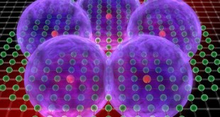
Advances in quantum mechanics have already led to innovations such as lasers and transistors. The next wave of quantum technology will result from the manipulation of quantum characteristics such as superposition and entanglement. Quantum technology (QT) applies quantum mechanical properties such as quantum entanglement, quantum superposition, and No-cloning theorem to quantum systems such as atoms, ions, electrons, photons, or molecules.
Quantum computing and quantum information processing are next revolutionary technology expected to have immense impact. Quantum computers will be able to perform tasks too hard for even the most powerful conventional supercomputer and have a host of specific applications, from code-breaking and cyber security to medical diagnostics, big data analysis and logistics.
Quantum Sensing exploit high sensitivity of quantum systems to external disturbances to develop highly sensitive sensors. They can measure Quantities such as time, magnetic and electrical fields, inertial forces, temperature, and many others. They employ quantum systems such as NV centers, atomic vapors, Rydberg atoms, and trapped ions.
Current atomic clocks based on Cesium or Rubidium loses just a second in 100 million years. These next generation Quantum clocks based on single atoms will lose only a second in a billion years. Quantum Gravimeters can measure gravity with greater sensitivity and reliability while more robust against external noise sources. Quantum navigation could be far more accurate than using current accelerometers and gyroscopes and will provide backup to GPS, if GPS fails or navigation in places where GPS is not available.
Currently, a wide range of different technological solutions are being investigated for these new applications, such as trapped ions, superconductors, quantum dots, photons and defects in semiconductors. Each technical solution has different pros and cons. Trapped ions have exquisite quantum properties but are challenging to integrate, whereas circuits of superconductors can be fabricated but can only operate at cryogenic temperatures. This is where materials like diamond come into play as they offer a compromise by being solid-state – making it easier to integrate into devices – and operational at room temperature.
Diamond has recently emerged as a unique material for quantum information processing. Diamonds are well-known gems but this material has been used in industry, as a tool for machining the latest smartphones, as a window in high-power lasers used to produce automotive components, and even as a speaker-dome material in high-end audio systems. However new applications of diamond are emerging in diamond quantum technologies.
In particular, Nitrogen-Vacancy (NV) centers in diamond exhibit quantum behavior up to room temperature. The diamond has many properties that fairly isolate the qubit from the surrounding environment including rigid structure, excellent heat conduction, and conducting electricity not at all. While silicon is traditionally used for computer and mobile phone hardware, diamond has unique properties that make it particularly useful as a base for emerging quantum technologies such as quantum supercomputers, secure communications and sensors.
The NV has an electron spin that is highly sensitive to magnetic fields, forming the basis for sensitive magnetometry. The electron spin can be detected and aligned by switching on a green LED on the material and measuring the intensity of the red fluorescence emitted. “It has been shown that NV electron spins can store quantum information for over 1s at room temperature,” said Twitchen.
“Diamond is an extraordinary material with such diverse properties that it is used in a wide range of applications, including smartphone processing, high-power lasers for automotive manufacturing and high-end audio systems. Now, thanks to continued technological advances, synthetic diamond materials with engineered levels of qubits made up of nitrogen-vacancy (NV) defects are paving the way for the next quantum magnetic sensing devices” said Daniel Twitchen, chief technologist at Element Six (E6).
Diamond Qubit
The reasons why diamond provides such a wonderful host to quantum defects come from its crystal structure. For example, diamond is a wide band-gap material, meaning that it can host a range of defects with transition energies in the optical regime, enabling the defects to be manipulated with readily available lasers. As carbon has a low atomic mass and very stiff interatomic bonds, it has a high Debye temperature (the temperature of a crystal’s highest normal mode of vibration), which makes the interaction of the NV centre with the vibrational modes of the surrounding lattice unusually weak, even at room temperature.
Diamond also has a naturally low concentration of nuclear spins (carbon-12 has a nuclear spin of 0 and there is only 1.1% carbon-13 (spin –1/2) in diamond). This reduces the likelihood of the quantum states “decohering”, when the spin is no longer in the desired state. Quantum states can also decohere via spin-orbit coupling – a relativistic effect where the spin of a charge interacts with its orbital motion. But because the NV defect has weak spin-orbit coupling, there is limited decoherence and the spin state lasts for longer.
Manufacturing Challenges
Together, these properties mean that it is possible to fabricate a diamond with a spin decoherence time of milliseconds at room temperature. And as well as diamond being a good host for spin defects, the NV centre is also particularly special in that its electronic energy-level structure means that the electronic spin associated with it can be manipulated simply by shining green light on it.
Despite these desirable features, the NV defect in diamond is not perfect. In an ideal world, all the photons emitted would be at 637 nm for them to be quantum mechanically indistinguishable. However, most of the photons emitted are at different wavelengths, from 637 nm to 800 nm, due to phonon interactions, which provides a challenge for some applications. Other difficulties are that diamond is not as easily processed as materials such as silicon – it is much harder to etch structures in diamond to improve optical collection from the defects, and high-purity single-crystal diamond has only been made up to around 10 mm2. These limitations of diamond and the NV defect have led to scientists looking for alternative defects in diamond and in other wide band-gap materials such as silicon carbide (SiC) and zinc oxide (ZnO). However, while a few other defects in diamond and other materials have been identified to have useful properties, no-one has found one that rivals diamond’s NV centres.
Meanwhile, many companies began developing new techniques to produce high-purity synthetic single-crystal diamond for industrial applications using microwave-assisted chemical vapour deposition. In the early 2000s, Element Six showed that it was possible to grow diamond with fewer than five impurity atoms per billion carbon atoms. In such diamond, nitrogen is the predominant impurity, and isolated NV centres can be probed. Eventually, in 2006 when this material’s quantum properties were tested, they were shown to be comparable to the Magic Russian Diamond. The finding was significant because the new synthetic diamond could be mass-produced and therefore allowed many more academic groups to have access to the material and start to understand how to control and use the NV defect.
Diamond qubit Manufacturing
“The ability to now make synthetic diamond with exceptional purity has unlocked the intrinsic qualities that make it the perfect host material for solid-state qubits,” Twitchen continued. He added, “a series of pioneering academic studies, initially at the Universities of Stuttgart and Harvard, demonstrated that NV color centers have a quantum spin which can be manipulated and read out at room temperature using simple, low-cost optical techniques, which generate exceptional quantum properties. NV centers are created by removing two adjacent carbon atoms from a diamond molecule and replacing one of them with a nitrogen atom, leaving a vacancy in the center.”
Mass producing Diamonds, reported in 2017
Scientists have developed a way to mass-produce tiny diamond crystals shaped like needles and threads, which may power next generation of quantum computing. Physicists from the Lomonosov Moscow State University in Russia have described structural peculiarities of micrometre-sized diamond crystals in needle and thread-like shapes, and their interrelation with luminescence features and field electron emission efficiency.
“The proposed technique involves determining formation of polycrystalline films from crystallites of elongate (columnar) shape,” Alexander Obraztsov, professor at the Lomonosov Moscow State University. For instance, ice on a surface of a lake often consists of such crystallites, which can be observed while melting,” said Obraztsov.
Meanwhile, many companies began developing new techniques to produce high-purity synthetic single-crystal diamond for industrial applications using microwave-assisted chemical vapour deposition. In the early 2000s, for example, staff at our firm Element Six showed that it was possible to grow diamond with fewer than five impurity atoms per billion carbon atoms, explain Matthew Markham and Daniel Twitchen physicists at Element Six, based in Oxford, UK. In such diamond, nitrogen is the predominant impurity, and isolated NV centres can be probed. Eventually, in 2006 when this material’s quantum properties were tested, they were shown to be comparable to the Magic Russian Diamond. The finding was significant because the new synthetic diamond could be mass produced and therefore allowed many more academic groups to have access to the material and start to understand how to control and use the NV defect.
The field of synthetic diamond science is moving very quickly, requiring us to develop CVD techniques that produce exceptionally pure synthetic diamond material with nano-engineering control,” said Bruce Bolliger, head of sales and marketing at Element Six Technologies.
Two research breakthroughs are poised to accelerate the development of synthetic diamond-based quantum technology, reported in May 2021
However there are two key problems; cost, and difficulty in fabricating the single crystal diamond layer, which is smaller than one millionth of a metre. A research team from the ARC Centre of Excellence for Transformative Meta-Optics at the University of Technology Sydney (UTS), led by Professor Igor Aharonovich, has just published two research papers, in Nanoscale and Advanced Quantum Technologies, that address these challenges.
“For diamond to be used in quantum applications, we need to precisely engineer ‘optical defects’ in the diamond devices — cavities and waveguides — to control, manipulate and readout information in the form of qubits — the quantum version of classical computer bits,” said Professor Aharonovich. “It’s akin to cutting holes or carving gullies in a super thin sheet of diamond, to ensure light travels and bounces in the desired direction,” he said.
To overcome the “etching” challenge, the researchers developed a new hard masking method, which uses a thin metallic tungsten layer to pattern the diamond nanostructure, enabling the creation of one-dimensional photonic crystal cavities. “The use of tungsten as a hard mask addresses several drawbacks of diamond fabrication. It acts as a uniform restraining conductive layer to improve the viability of electron beam lithography at nanoscale resolution,” said lead author of paper in Nanoscale, UTS PhD candidate Blake Regan.
To the best of our knowledge, we offer the first evidence of the growth of a single crystal diamond structure from a polycrystalline material using a bottom up approach — like growing flowers from seed. “It also allows the post-fabrication transfer of diamond devices onto the substrate of choice under ambient conditions. And the process can be further automated, to create modular components for diamond-based quantum photonic circuitry,” he said. The tungsten layer is 30nm wide — around 10,000 times thinner than a human hair — however it enabled a diamond etch of over 300nm, a record selectivity for diamond processing.
A further advantage is that removal of the tungsten mask does not require the use of hydrofluoric acid — one of the most dangerous acids currently in use — so this also significantly improves the safety and accessibility of the diamond nanofabrication process. To address the issue of cost, and improve scalability, the team further developed an innovative step to grow single crystal diamond photonic structures with embedded quantum defects from a polycrystalline substrate.
“Our process relies on lower cost large polycrystalline diamond, which is available as large wafers, unlike the traditionally used high quality single crystal diamond, which is limited to a few mm2” said UTS PhD candidate Milad Nonahal, lead author of the study in Advanced Quantum Technologies. “To the best of our knowledge, we offer the first evidence of the growth of a single crystal diamond structure from a polycrystalline material using a bottom up approach — like growing flowers from seed,” he added.
“Our method eliminates the need for expensive diamond materials and the use of ion implantation, which is key to accelerating the commercialisation of diamond quantum hardware” said UTS Dr Mehran Kianinia, a senior author on the second study.
Low-Cost Synthetic Diamond Fabrication, reported in June 2021
Using a thin tungsten layer as a restraining, conductive, removable hard mask, researchers at the University of Technology Sydney (UTS) developed a method for the fabrication of synthetic diamond. The developed material can be used for the photonic circuitry used in quantum technologies. The masking method is safe and inexpensive, and it uses the tungsten layer to pattern the diamond nanostructure that enables the creation of 1D photonic crystal cavities. Although the tungsten layer is only 30 nm wide, it can enable the creation of a diamond etch of over 300 nm.
“For diamond to be used in quantum applications, we need to precisely engineer optical defects in the diamond devices — cavities and waveguides — to control, manipulate, and read out information in the form of qubits,” professor Igor Aharonovich said. “It is akin to cutting holes or carving gullies in a super-thin sheet of diamond, to ensure light travels and bounces in the desired direction.”
With a tungsten layer (as opposed to a more conventional silicon oxide layer), the researchers achieved high levels of repeatability and reliability in their fabrication procedures, resulting in diamond cavities with quality factors approaching 1 × 10⁴. The researchers further showed that the cavities could be transferred onto a trenched substrate to allow for fully suspended diamond cavities.
“The use of tungsten as a hard mask addresses several drawbacks of diamond fabrication,” researcher Blake Regan said. “It acts as a uniform restraining conductive layer to improve the viability of electron beam lithography at nanoscale resolution. It also allows the post-fabrication transfer of diamond devices onto the substrate of choice under ambient conditions.”
The tungsten mask improves the safety and accessibility of the diamond nanofabrication process — the mask can be removed without having to use hazardous materials, such as hydrofluoric acid. The masking process can be further automated to create modular components for diamond-based quantum photonic circuitry, the researchers said.
To lower fabrication costs and improve scalability, the researchers also developed a way to grow single-crystal diamond photonic structures with embedded quantum defects from a polycrystalline substrate. In experiments, they used a pattern growth method to demonstrate how polycrystalline diamond could be used to grow single-crystal diamond structures with predefined shapes and sizes.
“Our process relies on lower-cost large polycrystalline diamond, which is available as large wafers, unlike the traditionally used high-quality single-crystal diamond, which is limited to a few square millimeters,” researcher Milad Nonahal said. “To the best of our knowledge, we offer the first evidence of the growth of a single-crystal diamond structure from a polycrystalline material using a bottom-up approach.”
Bottom-up approaches for the development of single-crystal diamond structures with purposely introduced color centers could be valuable for quantum technologies such as quantum supercomputers, secure communications, and sensors. The method developed by the UTS team could speed the development of diamond-based quantum technology. “Our method eliminates the need for expensive diamond materials and the use of ion implantation, which is key to accelerating the commercialization of diamond quantum hardware,” researcher Mehran Kianinia said. “This also significantly improves the safety and accessibility of the diamond nanofabrication process.”
U.S. Department of Energy’s (DOE) Argonne National Laboratory creates thin diamond membranes, reported in May 2022
In new research from the U.S. Department of Energy’s (DOE) Argonne National Laboratory, researchers have created extremely thin membranes of pure diamond. In a few locations in the crystal structure of the membrane, however, the team substituted carbon atoms with other atoms, notably nitrogen. These defects connect to neighboring atomic vacancies — regions where an atom is missing — creating unusual quantum systems known as “color centers.” Such color centers are sites for storing and processing quantum information.
“The defects in the diamond are interesting to us because they can be exploited for quantum application,” said Nazar Delegan, scientist in Argonne’s Materials Science division and the Pritzker School of Molecular Engineering at the University of Chicago and a collaborator with Q-NEXT. “Making these membranes allows us to integrate these defects with other systems and enables new experimental configurations.”
“Conventional diamond as a substrate is super hard to work with,” he said. “Our membranes are thinner and more accessible for a wide range of experiments.” The new diamond material fashioned by the researchers offers greater crystal and surface quality, enabling greater control over the coherence of the color centers.
“You can peel the membrane off and put it on a wide range of substrates, even put it on a silicon wafer. It’s a cheap, flexible and easy way of working with color centers without having to work directly with conventional diamond,” Guo said. “Because we’re able to control and maintain the quantum properties in individual defects within these very thin materials, it makes this platform promising as basis for a quantum technologies,” Delegan said.
Equipped with a way to cheaply and easily create diamond membranes that have robust color centers, scientists at Argonne hope to build a kind of assembly line for generating large numbers of these membranes for quantum experiments around the world.
Commercial Diamond manufacturing
Element Six, part of the De Beers Group, began offering a general-purpose quantum-grade CVD diamond in June 2020. E6 highlighted that this specialized diamond, which it calls DNV-B1, is an appropriate starting material for those interested in researching nitrogen-vacancy (NV) ensembles for quantum demonstrations, masers, detection of RF radiation, gyroscopes, sensing and further emerging applications, ranging from GPS-denied navigation to medical imaging.
“Diamond is an extraordinary material with such diverse properties that it is used in a wide range of applications, including smartphone processing, high-power lasers for automotive manufacturing and high-end audio systems. Now, thanks to continued technological advances, synthetic diamond materials with engineered levels of qubits made up of nitrogen vacancy (NV) defects are paving the way for the next quantum magnetic sensing devices” said Twitchen.
Quantum Diamond Technologies, Inc (QDTI) is a start-up that has spun out from Harvard University to make point-of-care diagnostics possible for diseases which require ultrasensitive detection of proteins in the early stages, such as heart conditions, cancer and Alzheimer’s. QDTI is exploiting diamond-enabled quantum systems, leveraging NV centers as the engine that will power our novel approach to biomolecule detection.
References and Resources also include:
https://www.sciencedaily.com/releases/2021/05/210517102648.htm
https://physicsworld.com/a/the-diamond-quantum%E2%80%AFrevolution/
https://www.photonics.com/Articles/Low-Cost_Synthetic_Diamond_Fabrication_Could_Step/a67053
https://www.eetimes.com/diamond-quantum-technology-for-medical-imaging/#
https://www.anl.gov/article/a-onestop-shop-for-quantum-sensing-materials