 International Defense Security & Technology Your trusted Source for News, Research and Analysis
Related Articles

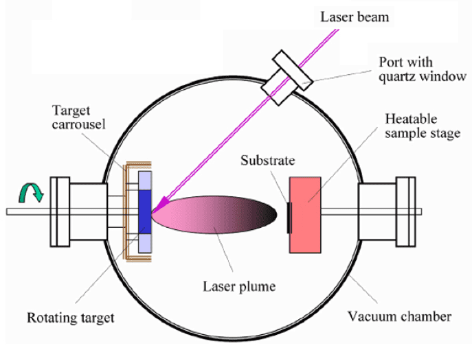
Pulsed laser deposition (PLD) is a physical vapor deposition (PVD) technique where a high-power pulsed laser beam is focused inside a vacuum chamber to strike a target of the material that is to be deposited. This material is vaporized from the target (in a plasma plume) which deposits it as a thin film on a substrate (such as a silicon wafer facing the target). This process can occur in ultra high vacuum or in the presence of a background gas, such as oxygen which is commonly used when depositing oxides to fully oxygenate the deposited films. The repetitive pulsing lays down a thin film of the material.
Pulsed laser deposition is only one of many thin film deposition techniques. Other methods include molecular beam epitaxy (MBE), chemical vapor deposition (CVD), sputter deposition (RF, magnetron, and ion beam). In 1987 when D. Dijkkamp, Xindi Wu and T. Venkatesan were able to laser deposit a thin film of YBa2Cu3O7, a high temperature superconductive material, which was of superior quality to that of films deposited with alternative techniques. Since then, the technique of pulsed laser deposition has been utilized to fabricate high quality crystalline films, such as doped garnet thin films for use as planar waveguide lasers. The deposition of ceramic oxides, nitride films,ferromagnetic films, metallic multilayers and various superlattices has been demonstrated. In the 1990s the development of new laser technology, such as lasers with high repetition rate and short pulse durations, made PLD a very competitive tool for the growth of thin, well defined films with complex stoichiometry.
Pulsed laser deposition can produce diamond-like coatings that make a surface nearly diamond-hard, or the process can apply high-temperature superconducting thin films to pave the way for practical superconducting devices. The technique also has the potential to radically enhance other devices, including electroluminescent displays and micro-optics.
The successful isolation of graphene (Gr) in the landmark work by Novoselov and Geim has heralded a plethora of 2D layered materials (2DLMs) that span chalcogenides, halides, nitrides, mono-/multi-elemental 2DLMs, as well as 2DLM-based heterostructures and composites. Despite the worldwide effort, researchers are still confronted with common challenges in material fabrication and device performance: How to garner high crystal quality and uniformity; how to scale up the growth; how to control the crystal orientation, thickness and morphology; how to optimize the device structures; how to achieve on-chip integration; how to maximize the photosensitivity; how to improve the repeatability.
To address these issues, researchers have been developing pulsed-laser deposition (PLD) for the synthesis of 2DLMs. Importantly PLD has enabled the actualization of large-area and high-quality 2DLMs owing to the following characteristics. (i) PLD is facile and precursor-free, which results in high efficiency and low contamination. (ii) Focused high-energy pulsed lasers endow the resulting plume with high activity. Thus, atoms from the plumes can migrate freely on substrates, which results in high uniformity and large growth area. (iii) PLD is a versatile deposition approach since the high-energy laser can decompose almost all condensed matter. This provides a solid foundation for the fabrication of complicated structures incorporating multiple 2DLM building blocks. (iv) The bombarded energetic atoms are beneficial to reduce the growth temperature. Thus, direct deposition of 2DLMs on flexible substrates, which are unsustainable at high temperature, is achievable.
Importantly, PDs based on PLD-grown 2DLMs have demonstrated competitive figures-of-merit to the commercial PDs, which offer great possibilities toward the next generation optoelectronics. Photodetectors (PDs) are devices that convert an optical signal to an electrical signal through a light-matter interaction. Photoelectric conversion is at the technical core of numerous applications such as imaging, optical communication, solar energy harvesting, remote sensing, photoelectric memory, environment monitoring and military reconnaissance.
Micro/nano structures have unique optical, electrical, magnetic, and thermal properties. Studies on the preparation of micro/nano structures are of considerable research value and broad development prospects. Several micro/nano structure preparation techniques have already been developed, such as photolithography, electron beam lithography, focused ion beam techniques, nanoimprint techniques. However, the available geometries directly implemented by those means are limited to the 2D mode. In recent years, the manufacture of conductive 3D structures on micrometers has caused great interest. Due to their potential applications in microelectronics, or applications in emerging fields such as flexible electronics, nanophotonics, and plasmons. Laser machining, a new technology for micro/nano structural preparation, has received great attention in recent years for its wide application to almost all types of materials through a scalable, one-step method, and its unique 3D processing capabilities, high manufacturing resolution and high designability. In addition, micro/nano structures prepared by laser machining have a wide range of applications in photonics, Surface plasma resonance, optoelectronics, biochemical sensing, micro/nanofluidics, photofluidics, biomedical, and associated fields.
PLD Technology
Only recently, though, have researchers mounted a strong attack on the technical problems holding pulsed laser deposition back from routine production use. While the basic setup is simple relative to many other deposition techniques, the physical phenomena of laser-target interaction and film growth are quite complex . When the laser pulse is absorbed by the target, energy is first converted to electronic excitation and then into thermal, chemical and mechanical energy resulting in evaporation, ablation, plasma formation and even exfoliation. The ejected species expand into the surrounding vacuum in the form of a plume containing many energetic species including atoms, molecules, electrons, ions, clusters, particulates and molten globules, before depositing on the typically hot substrate.
Several technical obstacles still stand between pulsed laser deposition and widespread commercialization. For instance, once a coating is applied to a substrate, it must adhere well throughout prolonged use of the product. This requirement is most demanding for the diamond-like coatings used to increase the hardness of heavy-duty parts such as bearings.
Simply applying diamond coatings to steel is impractical because the films delaminate in only a few rotations of a bearing. The problem is that the soft steel deforms under the hard film, breaking the adhesion. To cure this problem, researchers developed the concept of functionally graded coatings that blend gradually from pure metal to pure diamond; when coating titanium, a layer of the coating consists of a gradual shifting of titanium carbide composite to a pure diamond outer layer. Producing such coatings requires a hybrid device that uses pulsed laser deposition for the diamond and magnetron sputtering for the metal.
Another option involves multilayer coatings of materials such as titanium, titanium carbide, and diamond. While some hardness is lost, recent research has shown that multilayer graded coatings lasted more than a million cycles of wear against a sapphire ball, while a single layer of functionally graded coating lasted 100,000 cycles, and the simple diamond coating lasted only a few cycles.
One way to improve the hardness of diamond-like coatings in hybrid systems is to use a magnetic field. According to reports from the University of Hong Kong, the current in the plasma plume increases in magnetic fields of a few hundred to a couple of thousand Gauss. This result shows that more carbon ions are produced as electrons spiral around the magnetic-field lines, colliding with carbon atoms and stripping more electrons from them. With a higher current and more carbon ions, the binding of the carbon to the diamond-like films becomes more effective, and thus the hardness increases.
Another complication for pulsed laser deposition involves the production of doped thin films, which are often essential for high-temperature superconducting applications. Just premixing the materials makes changes in doping rates difficult, and doping can become nonuniform during deposition. At the National University of Singapore, researchers have designed a dual-beam approach to flexible and uniform doping. A laser beam is split into two and focused on two adjacent targets one for the film and the other for the dopant. A chopper placed in the way of the dopant beam allows continuous variation of the concentration of the dopant. When a different dopant is needed, the beam can simply be shifted to another nearby target.
Despite progress in overcoming technical obstacles to industrial application of pulsed laser deposition, the process is still constrained by economic barriers that face almost any new high-technology process. Producing reliable, consistent results requires process-monitoring techniques that are often beyond the resources of small company laboratories and university research teams. In addition, there is still no application with such clear near-term market potential that large companies are willing to invest substantial development funds. One promising possibility might be thin-film gallium nitride for blue-light-emitting laser diodes and LEDs, but, for now, industrial applications for pulsed laser deposition still lie in the future.
Laser controlled elemental composition of thin films and coating
Scientists at the Naval Information Warfare Center Pacific (NIWC-Pacific) have recently invented a technique to control the elemental composition of films deposited onto substrates using pulsed laser deposition (PLD). It can create more precise thin films and coatings for a wide variety of industries, including aerospace, automotive, and electronics.
In standard PLD, a small cylindrical target is ablated with focused laser pulses, which causes material from the target to become deposited onto a nearby substrate. Ideally, the target composition will be reproduced in the deposited film. In some cases, though, the resulting thin film can have a composition different from that of the target. For instance, a substrate heated to a very high temperature will cause more volatile elements to evaporate during the film growth process, leading to a smaller ratio of volatile elements to non-volatile elements when compared to the target.
To better control the composition of thin films, Navy researchers have developed a variation on PLD that improves on the method’s ability to grow thin layers of multi-component films. It involves a rotating, split ablation target with one half that contains more of the most volatile element being deposited. A laser beam is rastered across the target such that, over the course of the deposition, it spends more time on one half of the split target than on the other half. For example, the growth of a BiFeO3 film might have one target half with a 2:1 atomic ratio of bismuth (Bi) to iron (Fe), while the other half has a 1:1 atomic ratio of these elements. By spending more time on the bismuth-rich target side, the laser beam will ablate more bismuth, resulting in a film with a higher Bi:Fe ratio.
References and Resources also include: