Silicon, which has been a leading material in microelectronic industry for decades, is an attracting platform for photonic Integrated Circuits ( PICs ) thanks to transparency in the most widely used telecom wavelength bands, high refractive index contrast with cladding materials (SiO2, polymers, air), well-known processing conditions and production scalability (up to 12 inch wafers). However, expensive silicon-on-insulator (SOI) wafers are needed to fabricate devices with moderate insertion losses.
Comparing to inorganic materials, optical polymers are inexpensive, easy to process and flexible enough to meet a broad range of application-specific requirements. These advantages allow a development of cost-efficient polymer photonic integrated circuits for on-chip optical communications, signal processing, sensing, etc.
In the last years polymer photonics is witnessing a tremendous boost in research efforts and practical applications. Polymers are relatively inexpensive, can be engineered to exhibit unique optical and electronic or mechanical properties, and have demonstrated compatibility with various patterning methods. Extremely transparent and reliable optical polymers have been made commercially available for developing customer-specific photonic devices. The processing is usually fast and cost-effective. The real fascination of Polymer based photonics is that fact that it is very low power and is capable of very high data rates – both qualities that are critically needed by the community.
However, polymer platform suffers from some drawbacks, for example, low refractive index contrast between core and cladding. This limits light confinement in a core and, consequently, integrated polymer device miniaturization. Also, polymers lack active functionality like light emission, amplification, modulation, etc.
Polymer photonics
Polymers are solid organic materials consisting of many monomers linked to each other in a repetitive manner. Typically, polymers are highly transparent in visible and NIR region. Their refractive index ranges from 1.3 to 1.7 which is close to one of glasses. Low refractive index contrast between polymer core and cladding puts some limitation on the size of integrated polymer devices.
Polymers can be used as materials for photonic applications in several ways. First, polymers in themselves can possess useful optical properties such as electroluminescence, photoluminescence, or nonlinear optical properties. Second, polymers can act as matrices for optically active species, e.g. for dyes, liquid crystals (LCs), quantum dots, or metal nanoparticles. Third, polymers possessing topographic and/or compositional patterns can coherently scatter light. Finally, polymer templates are routinely used for producing photonic materials.
Due to its flexibility and broad compatibility, polymers can be integrated in various photonic platforms such as SOI, III-V and silica PLCs, or vice versa, photonic components made from a multitude of materials can be integrated in a heterogeneous / hybrid manner on polymer platform.
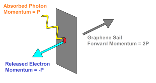
Another advantage of polymers is a possibility to combine it with graphene, to dope with semiconductor nanoparticles or organic chromophores for active applications like light emission, amplification or electro-optic modulation. This significantly broadens functionality of integrated photonic devices based on polymer platform.
Development of polymer materials for photonic applications will include the synthesis of polymers with high refractive indexes and/or useful optical and electronic properties (for instance, using inorganic polymers), the use of optically active hybrid polymer-inorganic materials, and the utilization of materials with multiple sensing functions. Specific functionalities of polymers and rapid dynamic response to particular, and sometimes multiple, external stimuli will serve as another criterion for the successful commercialization of photonic polymer materials.
Nanostructured polymers for photonics
In particular, interaction of light with materials possessing a periodic modulation in their structure has led to a range of interesting and sometimes unique effects, which have shown promising applications in the production of Bragg mirrors, switches, filters, superprisms, waveguides, and optical resonators.
Owing to the ability to combine structure- and composition-dependent properties, the scope of research in polymer nanostructured materials with periodic structures has rapidly expanded beyond traditional polymer nanocomposites for optical applications. Future advances in this area of science and technology will aim at improving the photonic functionalities of polymer materials, controlling structural defects, and integrating photonic devices.
Polymer Photonics Applications
Many Satellite payloads require micro-component optical or photonic systems including Micro Electro-Mechanical Systems (MEMS) devices, Interferometric Fiber-Optic Gyroscopes (I-FOG), ring laser gyros, integrated monolithic photonics and new, innovative, miniaturized, cost-effective, reliable and radiation-resistant sensor and communications technologies. Many Space missions rely on optical and photonic technologies, including directed-energy planetary defense, directed-energy spacecraft propulsion, active target illumination, orbital debris mitigation, spectrometry and other missions.
In the space environment, the effects of ionizing radiation, temperature ranging, and environmental effects such as atomic oxygen (AO), vacuum, and ultraviolet (UV) radiation can degrade space sensors, systems, and related components.
Biological and polymer-based photonics both linear and nonlinear, hybrid-inorganic-organic/polymer technologies have potential applications in implementation of hardened nano-, micro-, and macro-photonic components and systems such as: optical fibers, fiber gratings, fiber amplifiers, and fiber lasers as well as optical sensors, optical data buses, solar cells, high- and low-power laser sources, detectors, modulators, couplers, optical interconnects, multiplexers-demultiplexers, signal processing systems, guidance systems, targeting, radar, imaging, optical communications, optical limiter materials and components.
Polymer nanostructured materials for secure data storage is another field of research that holds promise, with an increasing demand for the protection of identification documents, credit cards, and authentication labels against counterfeiting. Here, future advances depend on the synthesis of photostable chromophores, the incorporation of multiple security features in polymer recording media, and the ability to integrate polymer security materials with cost-effective optical reading devices.
Fabrication
Optical polymers possess several advantages that make them attractive for photonic integration. First, high quality thin films can be deposited with inexpensive spin-coating techniques routinely used in microelectronic industry. Desired film thickness is easily obtained by changing polymer solution viscosity and/or adjusting spin-coating speed. In this way, polymer films can be obtained within several minutes without any use of expensive deposition techniques such as physical vapor deposition (PVD), epitaxy, etc.
Fabrication of photonic crystal and nonlinear photonic crystal is a key parameter for modern optics with numerous applications in different fields. Researchers of Molecular Quantum Photonics Laboratory propose a powerful fabrication technique based on the interference of two laser beams with multiple exposures. This technique allows to imprint different kinds of periodic and quasi-periodic structures into polymer materials. This fabrication technique allows to realize very structures in a very short fabrication time.
“The technique can be applied for different kinds of polymer materials, passive or active. When using a specific quasi-periodic structure, we could directly obtain a polymer-based photonic crystal with a good photonic bandgap as the one obtained with semiconductor material. In particular, when using nonlinear polymer material, we could obtain the so-called nonlinear photonic crystals, which are very interesting for many applications, such as generation of new waves by frequency conversion, high speed optical switching, low threshold laser, etc,” write authors.
These polymer-based photonic structures could also be transfered to other materials, such as metallic and magnetic materials, which allow to study other physical effects, such as plasmonics and magneto-optics, offering numerous interesting applications.
LightWave Logic Develops Polymer Photonics Technology Platform
Electro-optical technology provider Lightwave Logic Inc. is developing a polymer photonics technology platform to meet scaling metrics dictated by large data centers, telecommunications system operators and networking companies.
Polymers are so-called spin-on materials. They can be spun onto InP as well as SiP (even GaAs) PICs to create very high performance, very low power integrated photonics solutions. The polymers that Lightwave Logic have created exhibit high temperature stability. So, they are ideally suited for the heavy data applications markets such as datacenters – as well as high performance computing.
Lightwave’s component library includes slot waveguide modulators, ridge waveguide modulators, passive waveguides and waveguide splitters, and will now be expanded to include multiplexers, demultiplexers and spot-size converters, necessary for telecom and datacom devices.
The combination of Polymer Photonics with a silicon platform, such as a slot waveguide modulator coated with a thin coat polymer as the active component, will enable photonics to grow in integration density faster than before, beyond 1,000 photonics devices on a single chip. The components are low-cost and high-performance, allowing for high integration scaling design-rules.
“We continue to make steady progress in the development of our Polymer Photonics technology platform and are on track to achieve our stated goal to have our first demonstration device completed by the end of this year,” said Tom Zelibor, chairman and CEO of Lightwave Logic.
Lightwave Logic (LWLG) is commercializing it’s P2ICTM organic polymer systems for a variety of electro-optic devices.Our company has already demonstrated 50Gbps capable modulators for integrated photonics and plans to further develop its P2IC® (polymer PIC) platform over the next few years, said its CEO.
Lightwave Logic produces prototype electro-optic demonstration devices and is moving toward the commercialization of its high-activity, high-stability organic polymers for applications in electro-optical device markets.
Conclusion
The large bandwidth, low drive voltages and ease of integration of polymeric electrooptic materials provide a strong argument of utilization. The adoption of polymeric modulators will require that they meet thermal and optical power handling before they displace an established lithium niobate.
References and Resources also include:
http://www.photonics.com/Article.aspx?AID=60854
http://www.sciencedirect.com/science/article/pii/S1369702108700567
https://www.diva-portal.org/smash/get/diva2:1163572/FULLTEXT01.pdf
 International Defense Security & Technology Your trusted Source for News, Research and Analysis

