International Defense Security & Technology Your trusted Source for News, Research and Analysis
Related Articles
Photodetectors, also called photosensors, are sensors of light or other electromagnetic radiation. There is a wide variety of photodetectors that may be classified by mechanism of detection, such as photoelectric or photochemical effects, or by various performance metrics, such as spectral response. Photodetectors are devices that measure photon flux or optical power by converting optical signals into electrical current through electronic processes.
Infrared photodetectors (IRPDs) have become important devices in various applications such as night vision, military missile tracking, medical imaging, industry defect imaging, environmental sensing, and exoplanet exploration. IR radiation can generally be divided into different categories, namely near-wavelength region from 0.8 to 3 μm, mid-wavelength IR (MWIR) region from 3 to 5 μm, and long-wavelength IR (LWIR) region from 8 to 12 μm. The MWIR and LWIR regions are most important for free-space communications and astronomy since the high transparency of the atmosphere at these wavelengths allows transmission without significant losses.
The same regions are also widely used for night vision and missile tracking for military applications. Portable infrared cameras based on these can see invisible wavelengths of light have long been used by law enforcement, soldiers, firefighters, and others to see in the dark or locate people by the body heat they emit. IR detection also enables many non-contact, non-destructive inspection methods that are widely utilized in industry, such as automotive and defect detection in electronic circuits. IR detection has similarly found many medical applications.
Principally, the mechanism of photodetection includes three processes: (1) generation of carriers by incident light, (2) carrier transport or multiplication through the current-gain mechanism, and (3) extraction of carriers as terminal current to provide the output signal. We can categorize the photodetectors by various structural and operational parameters.
The two main types of IR detectors are thermal detectors and photodetectors. In a thermal detector, the incident IR photons are absorbed by a thermally isolated detector element, resulting in an increase in the temperature of the element. The temperature is sensed by monitoring an electrical parameter such as resistivity or capacitance. In a quantum or photon detector, electromagnetic radiation absorbed in a semiconductor material generates electron-hole pairs (EHP), which are sensed by an electronic readout circuit (ROIC). The response time and sensitivity of a photodetector can be higher, but they generally have to be cooled in order to cut thermal noise.
Semiconductor-based photodetectors typically have a p–n junction that converts light photons into the current. The absorbed photons make electron-hole pairs in the depletion region. Photodiodes and phototransistors are a few examples of photodetectors. The photodetector performance (detectivity bandwidth product) can be enhanced by two methods. The first method is based on engineering the electronic properties of the absorbing material for improved figures of merits such as detectivity and quantum efficiency. The second method is based on increasing the coupling of light to the electronic states of the absorbing material.
Although conventional semiconductors are of great advantages for the fabrication of photodetectors, there are some limitations for implementation in modern devices. One of the most challenging issues associated with Si (dominated material in solid-state electronics and photonic devices in last four decades) is the intrinsic bandgap which restricts the photoresponsivity of the device to specific light bandwidth. Silicon and cadmium sulfide (CdS) nano-ribbon photodetectors can be used mainly for detection in the visible regime of the electromagnetic spectrum; gallium sulfide (GaS) nanosheet and molybdenum disulfide (MoS2) enables the detection in ultraviolet and infrared regimes,
respectively. Small bandgap semiconductor compounds such as mercury cadmium telluride (HgCdTe), lead sulfide (PbS) or lead selenide (PbSe) were used for the detection of mid-infrared photons, and in the far-infrared regime, thermal sensing techniques are utilized.
In addition to the limitations associated with the bandwidth, the speed of response in conventional photodetectors is limited by capacitative effects, the trapping of charge carriers, and the saturation speed of carriers which suppress the response of the photodetector in the
high-frequency domain.
Mature semiconductor technologies such as mercury cadmium telluride and III–V material-based photodetectors have been dominating the industry. However, in the last few decades, significant funding and research have been focused to improve the performance of IRPDs such as lowering the fabrication cost, simplifying the fabrication processes, increasing the production yield, and increasing the operating temperature by making use of advances in nanofabrication and nanotechnology.
Graphene photodetectors
As an exotic 2-dimansional (2D) material, graphene is an attractive material for future optoelectronic devices due to its excellent electronic
and optical properties, such as variety of transport phenomena that are characteristics of 2D Dirac fermions, near-ballistic transport at room
temperature, bipolarity, high purity, high mobility, high critical current density, linear dispersion of the Dirac electrons, and saturable absorption.
With linear dispersion near the Dirac point and various forms of light-matter interaction, graphene offers a high optical responsivity in a broad spectral range. In particular, Graphene-based photodetectors are capable of detecting the entire spectrum, from infrared to visible to ultraviolet, and in the future would lead to ultrasensitive detectors and that too at room temperature. Second, graphene exhibits extremely high carrier mobility up to ∼106 cm2/V·s and is capable of ultra-fast operation and process images faster than existing photodetectors. The detector is also more sensitive to low levels of light than current technology.
Graphene detectors can be divided into two categories: either photon and thermal (the bolometer effect) detectors. The majority of graphene pristine photodetectors exploit graphene metal junctions, graphene p-n junctions, and FET transistors. Most graphene photodetectors utilize graphene-metal (or semiconductor) junctions, or graphene p-n junctions to spatially separate and extract photon-generated carriers. The development of the graphene high responsivity photodetectors is determined by the two major challenges: the low optical absorption in the detector’s active region (~100–200 nm) and short photocarrier lifetime meaning that graphene photodetectors are mainly limited by the trade-off between high responsivity, ultrafast time response and broadband operation.
Responsivity measures the input-output gain of a detector system. In the specific case of a photodetector, responsivity measures the electrical output per optical input. The responsivity of a photodetector is usually expressed in units of either amperes or volts per watt of incident radiant power. For a system that responds linearly to its input, there is a unique responsivity. For nonlinear systems, the responsivity is the local slope. Many common photodetectors respond linearly as a function of the incident power
However, the reported maximum responsivity of photodetectors based on the above-mentioned pure graphene junctions is lower than 10 mA/W. Monolayer graphene absorbs 2.3% of the incident light, remarkably high for a material with only one atom thickness, but still very low in absolute terms. As a gapless semiconductor, graphene generates a large dark current. Meanwhile, the lifetime of photocarriers in graphene is very short ∼1 ps. Graphene functionalization and artificial nanostructures have been utilized to introduce bandgap and mid-gap states into graphene for increasing the lifetime of photocarriers. However, this sacrifices the intrinsic high carrier mobility, which seriously restricts the response speed of graphene photodetectors.
Double-layer graphene tunneling devices have demonstrated high responsivity from visible to near-infrared spectrum. However, the response speed is limited by the trapped photocarrier lifetime in the tunnel barrier. Graphene photodetectors coupled with waveguides, microcavities, plasmonic structures and optical antennas have been realized with high responsivities by increasing the light-matter interaction length in graphene. However, the bandwidth of such photodetectors is limited by the resonant wavelength of the nano-photonic structures.
Graphene based bolometers are faster, simpler, and covers more wavelengths.
Researchers from MIT, Harvard University and Army Research Laboratory have integrated graphene based photo thermo-electric detectors with micro machined silicon nitride membranes, thereby enabling detection as well as stand-off imaging of an incoherent blackbody target (300–500 K) such as normal person at room temperature without cryogenic cooling.
The Current technologies, such as high performance photon based detectors (i.e., HgCdTe), often require cryogenic cooling to mitigate noise sources such as thermally excited carriers or stray blackbody optical photons. These drawbacks can be avoided at infrared wavelengths by using thermal detectors that offer higher sensitivities at 300 K. “Therefore, in this work we leverage graphene’s band structure not for optical detection but rather thermal detection in the mid-infrared,” according to authors.
Researchers Dmitri Efetov, Professor Dirk Englund of MIT’s Department of Electrical Engineering and Computer Science, Kin Chung Fong of Raytheon BBN Technologies, and colleagues from MIT and Columbia University have developed a new type of bolometer that is faster, simpler, and covers more wavelength, can work at room temperature — and may be much less expensive.
In their paper, Graphene-Based Thermopile for Thermal Imaging Applications, they reported that they created the device, by integrating graphene with silicon microelectromechanical systems (MEMS). The resulting infrared sensors were small enough that they could be “integrated in every cellphone and every laptop,” according to the study’s co-author, Tomas Palacios. “They could one day be integrated into car windshields, giving you “night-vision systems in real time without blocking a driver’s regular view of the road,” he further said.
The device is entirely different from traditional bolometers, which typically use a metal to absorb the radiation and measure the resulting temperature rise. Instead, this team developed a new type of bolometer that relies on heating electrons moving in a small piece of graphene, rather than heating a solid metal. The graphene is coupled to a device called a photonic nanocavity, which serves to amplify the absorption of the radiation, Englund explains. “We believe that our work opens the door to new types of efficient bolometers based on low-dimensional materials,” says Englund, the paper’s senior author. He says the new system, based on the heating of electrons in a small piece of a two-dimensional form of carbon called graphene, for the first time combines both high sensitivity and high bandwidth — orders of magnitude greater than that of conventional bolometers — in a single device.
The new bolometer they built, and demonstrated under laboratory conditions, can measure the total energy carried by the photons of incoming electromagnetic radiation, whether that radiation is in the form of visible light, radio waves, microwaves, or other parts of the spectrum. That radiation may be coming from distant galaxies, or from the infrared waves of heat escaping from a poorly insulated house.
“Most bolometers rely on the vibrations of atoms in a piece of material, which tends to make their response slow,” he says. In this case, though, “unlike a traditional bolometer, the heated body here is simply the electron gas, which has a very low heat capacity, meaning that even a small energy input due to absorbed photons causes a large temperature swing,” making it easier to make precise measurements of that energy. Although graphene bolometers had previously been demonstrated, this work solves some of the important outstanding challenges, including efficient absorption into the graphene using a nanocavity, and the impedance-matched temperature readout.
The authors achieved large responsivities at the room temperature (order of ∼7–9 V/W at λ = 10.6 μm), with a time constant of ∼23 ms. “The new device is very sensitive, and at the same time ultrafast,” having the potential to take readings in just picoseconds (trillionths of a second), says Efetov, now a professor at ICFO, the Institute of Photonic Sciences in Barcelona, Spain, who is the paper’s lead author. “This combination of properties is unique,” he says.
The new system also can operate at any temperature, he says, unlike current devices that have to be cooled to extremely low temperatures. Although most actual applications of the device would still be done under these ultracold conditions, for some applications, such as thermal sensors for building efficiency, the ability to operate without specialized cooling systems could be a real plus. “This is the first device of this kind that has no limit on temperature,” Efetov says.
The findings, published in the journal Nature Nanotechnology, could help pave the way toward new kinds of astronomical observatories for long-wavelength emissions, new heat sensors for buildings, and even new kinds of quantum sensing and information processing devices, the multidisciplinary research team says.
The new technology, Englund says, “opens a new window for bolometers with entirely new functionalities that could radically improve thermal imaging, observational astronomy, quantum information, and quantum sensing, among other applications.” For astronomical observations, the new system could help by filling in some of the remaining wavelength bands that have not yet had practical detectors to make observations, such as the “terahertz gap” of frequencies that are very difficult to pick up with existing systems. “There, our detector could be a state-of-the-art system” for observing these elusive rays, Efetov says. It could be useful for observing the very long-wavelength cosmic background radiation, he says.
Daniel Prober, a professor of applied physics at Yale University who was not involved in this research, says, “This work is a very good project to utilize the many benefits of the ultrathin metal layer, graphene, while cleverly working around the limitations that would otherwise be imposed by its conducting nature.” He adds, “The resulting detector is extremely sensitive for power detection in a challenging region of the spectrum, and is now ready for some exciting applications.”
And Robert Hadfield, a professor of photonics at the University of Glasgow, who also was not involved in this work, says, “There is huge demand for new high-sensitivity infrared detection technologies. This work by Efetov and co-workers reporting an innovative graphene bolometer integrated in a photonic crystal cavity to achieve high absorption is timely and exciting.”
Graphene Photodetector Demonstrates Speed, High Responsivity
Researchers from University of California, Los Angeles (UCLA) fabricated the photodetector using photoconductive nanostructures based on gold-patched graphene nanostripes. They laid stripes of graphene over a silicon dioxide layer; then they created a series of comb-shaped nanoscale patterns made from gold, with “teeth” about 100 nm wide. The graphene nanostripes act as a net to catch incoming photons. The graphene then converts the photons into an electrical signal. The gold comb-shaped nanopatterns quickly transfer that information into a processor, which produces a corresponding high-quality image, even under low-light conditions.
The graphene photodetector demonstrated high-responsivity (ampere per watt; A/W) photodetection from the visible to the IR regime of 0.6 A/W at 0.8 μm, and 11.5 A/W at 20 μm, with operation speeds exceeding 50 GHz. The results indicate an improvement of the response times by more than seven orders of magnitude and an increase in bandwidths of one order of magnitude, compared to higher-responsivity graphene photodetectors based on quantum dots and tunneling barriers.
“We specifically designed the dimensions of the graphene nanostripes and their metal patches such that incoming visible and infrared light is tightly confined inside them,” said researcher Semih Cakmakyapan. “This design efficiently produces an electrical signal that follows ultrafast and subtle variations in the light’s intensity over the entire spectral range, from visible to infrared.”
The team believes that the combination of broadband and ultrafast photodetection with high responsivity could have an impact on future hyperspectral imaging and sensing systems. Researchers said that to further enhance performance, the symmetric gold patches could be replaced with asymmetric metal patches; this could lead to symmetry breaking and enable bias-free, low-dark-current device operation.
Chinese Researchers produce Graphene photodetectors using Photogating effect
Photogating effect could be simply understood as the prolonged photocarrier lifetime induced by trap states at defects or impurities. These localized states can trap holes/electrons and act as a local gate, effectively modifying the conductance of the channel material. Marcus et al. observed that the visible light absorption in the heavily p-doped Si substrate generates a photovoltage to gate the carbon-nanotube transistors and results in a significant enhancement of photocurrent. Similar mechanisms have been applied to graphene photodetectors but using lightly p-doped Si substrates. Such photogating effect allows graphene photodetectors with both high responsivity and high bandwidth. Experimental investigations of responsivity enhanced by the photogating effect still need more efforts to gain deeper understanding of the microscopic mechanisms of graphene photodetectors. For example, one would naturally raise a question whether the Si substrate has to be lightly p-doped or not.
In 2018, The authors from National University of Defense Technology, investigated the photogating effect in graphene photodetectors by utilizing heavily n-doped Si/SiO2 as substrate. their experiment demonstrated room temperature graphene photodetectors with high responsivity from visible (∼500 A/W at 450 nm) to near-infrared (∼4 A/W at 1064 nm). The measured photocurrent changes with applied gate voltage and exhibits a nonlinear dependence on the laser power, consistent with the photogating effect.
“The large photocurrent and high responsivity are attributed to the light absorption in heavily n-doped Si/SiO2 oxide substrate. The electric field due to the band bending at the Si/SiO2 interface effectively separates the photon-induced electron-hole pairs in Si. The accumulation of holes at the Si/SiO2 interface acts as an additional gate, resulting in a horizontal shift in the transfer curve and thus generating a significant photocurrent in graphene. The photocurrent changes with applied gate voltage and rapidly increases with laser power at low intensity and saturates at high intensity, showing a clear nonlinear behavior. Furthermore, we found that the photoresponse of graphene transistors has a cut-off wavelength of ∼1100 nm, consistent with the absorption spectrum of Si. Compared with hybrid graphene devices of similar responsivity but complicated structures, our graphene photodetectors exhibit much simple architectures, paving a way for Si-compatible applications such as on-chip optical communications.”
Graphene photodetectors for Infrared Contact Lens
Researchers at the University of Michigan turned their glasses into a reality, using graphene to develop fingernails-sized infrared image sensors without the need for bulky cooling devices. Because of its small size, light weight, it can be integrated into contact lenses or mobile phones, in the military, security, medicine and other fields have a wide range of applications
Michigan researchers utilized optical capabilities of graphene to create an infrared contact lens. Graphene is capable of detecting the entire spectrum, from infrared to visible to ultraviolet, however, being only a single atom thick, it can absorb only 2.3 percent of light.
The researchers have created a new device by sandwiching an insulator between two sheets of graphene. By measuring the change in the flow of current in the bottom layer, the researchers could derive just how much light hit the top layer. This contact lens sized device has very nearly the same sensitivity as cooled mid-infrared detectors, and that too at room temperature.
When the light hits the top graphene, the device releases electrons and creates a positively charged hole. Then, under the quantum tunneling effect, electrons pass through the middle insulating layer and reach the bottom of the graphene layer. At this point, the positively charged holes remaining on the upper graphene will produce an electric field and affect the current of the lower graphene. By measuring the change of the current, the brightness of the light irradiated on the upper graphene can be inferred. Chong said the new method first allowed the sensitivity of both the IR and far-infrared sensors to a new height that could be comparable to a traditional infrared sensor that required a cooling device to run.
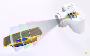
Transparent graphene photodetectors make advanced 3D camera
A new 3D camera made from a stack of transparent graphene photodetectors can capture and focus on objects that are different distances away from the camera lens. The device, made by researchers at the University of Michigan in the US, might find use in applications as diverse as biological imaging, driverless cars and robotics.
Most of today’s optical imaging systems use a flat optical detector to record the intensity of light reflected from an object at each pixel. However, since these systems detect light in only one plane, all the information concerning the direction of the light rays is lost. This means that the recorded images are simple 2D projections of the actual 3D object being imaged. The images acquired thus have a finite field depth – that is, objects at only a particular distance from the camera are in sharp focus, and items in front or behind that distance are out of focus and appear blurred. What is more, because of the 2D projection, it is impossible to determine how far away each object is from the camera.
An ideal imaging system would overcome this problem by producing a complete representation of the 3D scene with an infinite depth of field in a single exposure. Such a device could be made of different detector arrays, each stacked along the path of the different incoming light rays. By then detecting multiple focal planes of data all at the same time, algorithms could be used to reconstruct a complete (“light field”) image of the scene in three dimensions, with each object in the scene being in focus. Furthermore, the distance to each object could be determined. Such range detection, as it is known, would be extremely useful for applications like driverless cars and robots.
A team of researchers led by Zhaohui Zhong, Jeffrey Fessler and Theodore Norris of the Department of Electrical Engineering and Computer Science at the University of Michigan have now succeeded in building such a photodetecting device. Their new 3D camera uses a stack of transparent sensors made from graphene (a sheet of carbon atoms just one atom thick that has excellent optical transmittance in the visible and near‐infrared range) to simultaneously capture images that are focused to different distances from the camera lens.
The researchers fabricated their photodetector on a transparent glass substrate (rather than the silicon chips usually employed in such devices) using graphene as the light-sensing layer, the conducting channel layer, the gate layer and even the interconnects (which are usually made of metal). Using graphene for all the different functional components of the device in this way allows for sensitive light detection and a transparency of around 95%.
To prove that their design works, the researchers built a single-pixel focal stack light field camera comprising a 100 mm focal length front imaging lens and two single-pixel graphene photodetectors separated by 2 mm. The test object was a point source formed by an illuminated 30-micron-sized pinhole. The point source, the centre of the imaging lens and the two photodetectors were all aligned along the same optical (z) axis.
Range detection
When the point source is far from the lens, the image produced is completely out of focus on both graphene detectors. However, when the researchers then move the point source towards the lens, it becomes perfectly focused on the front detector while remaining out of focus on the back detector. “As we continue to move the point source towards the imaging lens, the intensity of the image decreases on the front detector and increases on the back detector,” the researchers explain. “At some point, the test object is sharply imaged on the back detector while staying out of focus on the front one.”
By knowing the lens focal length and the positions of the detectors, the researchers say they can determine the distance of the object from the lens. Likewise, knowing the light intensity profile along the z axis allows them to calculate the 3D depth information of the scene from the data using image processing algorithms.
While their current graphene sensors do not have high enough resolution to depict actual images at present, the researchers have simulated how larger sensor arrays arranged in their set-up might capture a scene (see figure above). They say they have also developed the algorithms required to perform such image reconstructions from transparent focal stack data.
As well as applications in autonomous driving and robotics, the new photodetectors, which are detailed in Nature Photonics, might also be ideal for biological imaging in cases where it is important to image 3D volumes, the Michigan team tell Physics World. “There are many applications in optical ranging and object identification that may not require the full computational reconstruction of 3D objects and we are currently pursuing this line of work,” they add.
Graphene-Based Tracking System May Streamline Autonomous Vision, reported in May 2021
A real-time 3D tracking system developed at the University of Michigan may one day replace lidar and cameras in autonomous technologies. The system combines transparent graphene-based light detectors and advanced neural networks to sense and image scenes in three dimensions. The graphene photodetectors, developed by Zhaohui Zhong, associate professor of electrical and computer engineering, were modified to absorb only about 10% of the light to which they are exposed, which makes them nearly transparent. Due to graphene’s high sensitivity to light, that percentage is sufficient to generate images that can be reconstructed through computational imaging.
“One way to make transparent detectors is to make the absorbing material thin, usually below tens of nanometers,” Dehui Zhang, a doctoral student in electrical and computer engineering, told Photonics Media. “The trade-off is less absorption and weaker response.” Traditional image sensors based on silicon and III-V materials, Zhang explained, target high absorption to maximize response, and are therefore not transparent. “We solve the problem by using atomically thin 2D materials to fabricate phototransistors,” Zhang continued. “The photoconductive gain amplifies the small signal from the weak absorption, which enables a large response and high transparency simultaneously.”
The photodetectors in the new design are stacked behind one another, creating a compact system with each layer focused at a different focal plane to enable 3D imaging. “The in-depth combination of graphene nanodevices and machine learning algorithms can lead to fascinating opportunities in both science and technology,” Zhang said. “Our system combines computational power efficiency, fast tracking speed, compact hardware, and a lower cost compared with several other solutions.”
In addition to 3D imaging, the researchers also used the system for real-time motion tracking, critical to a variety of autonomous robot applications. To do this, they had to find a way to determine the position and orientation of an object being tracked. Typically this is done with lidar and light-field cameras, both with significant limitations, the researchers said. Other approaches use metamaterials or multiple cameras. “The speed can be fast given the small data size of focal stack images and the short inference time of neural networks using GPU,” Zhang told Photonics Media.
The technology possesses certain advantages over other modalities, which themselves have particular strengths and weaknesses, Zhang said; lidar, for example, requires active illumination, which results in extra power consumption, complexity, and safety concerns. Light-field imaging takes in a great amount detail, though it can bog down speed due to the large amounts of data that has to be processed. Another approach, stereo cameras, can be bulky due to the necessity of multiple cameras.
The team found that the technology could be used for motion tracking with the addition of deep learning algorithms. Doctoral student Zhen Xu helped to bridge the gap between the two fields. Xu built the optical setup and worked with the team to enable a network to decipher positional information.
The network is designed to search for specific objects within the scene, and then to focus only on the object of interest, such a pedestrian or an object moving into a driver’s lane on the highway. The technology works particularly well for stable systems, such as in automated manufacturing or in certain medical contexts. “The algorithm was implemented and trained by Pytorch by feeding the network training samples,” Zhang said. “In the case of 3D point object tracking, each training sample consists of an input focal stack and the corresponding 3D coordinates of the point object being imaged.”
The samples were either collected experimentally using the transparent graphene detector in a single exposure, Zhang said, or with a CMOS camera with multiple exposures each with a distinct focus position. In a demonstration, the technology successfully tracked a beam of light, and a ladybug, using a stack of two 16-pixel graphene photodetector arrays. The researchers also demonstrated that the method is scalable, and they believe that it would take as few as 4000 pixels for some practical applications, and 400- × 600-pixel arrays for many more.
DARPA Awards for Graphene IR Detector development
In June 2016 DARPA awarded a $1.3 million grant to a team led by University of Central Florida researcher Debashis Chanda to fund the development of a next-generation IR detector that could be used in night vision, meteorology and space exploration.
The team is working on an entirely new type of detector that relies on thin graphene, a one-atomic-layer thick, 2D material. Chanda envisions an infrared detector that is small, portable, doesn’t need to be cooled and produces high-resolution images. Unlike current technologies, which can detect only one band of light, the next-gen detector would be tunable and able to see a range of bands.
More powerful infrared detectors that produce more detailed images – ones typically used by NASA and defense agencies – are large, expensive and can only function at ultra-low temperatures. “The biggest problem is that most infrared detectors need cryogenic cooling, and in most cases you can’t carry a big cooling tank with you,” Chanda said. “That is a big barrier.”
“We came up with the idea that one can make graphene to strongly absorb light in the infrared domain and we showed that we can also tune the response electronically,” Chanda said. “If you can take an infrared image in different spectral bands, you can extract much more information.” The team intends to collaborate with defense majors such as Northrop Grumman, Lockheed Martin and St. Johns Optical Systems for integration and packaging.
In Jan 2022, DARPA funded for the three-year, DARPA Direct Phase-II project will be split between UCF and E-Skin Displays Inc., which is a California startup focused on commercializing technologies developed in Chanda’s lab. The main goal of the new grant is to take this new concept to the commercialization domain by transforming it to a functional infrared camera.
The project will use a new infrared detection concept based on graphene — a material that is composed of one atom thick regular honeycomb arrangement of carbon atoms. “We could pattern graphene with engineered nano-scale features that works as nano-antennas to collect light —enhancing infrared light absorption by over 30 times compared to the bare graphene sheet,” says Debashis Chanda, the project’s leader and a professor in UCF’s NanoScience Technology Center. “This enables this ‘engineered’ graphene to be used as a light detection material.”
The new imaging system will be more sensitive than current infrared imaging systems and will cost significantly less as it will not require expensive and cumbersome cryogenic cooling. “A highly sensitive, room temperature infrared imaging system will facilitate many practical applications to emerge,” Chanda says. “The next challenge is to add required electronics to convert this new one-atom thick material to a functional camera.”
References and Resources also include:
http://news.mit.edu/2018/better-device-measuring-electromagnetic-radiation-0611
https://www.photonics.com/Articles/Graphene_Photodetector_Demonstrates_Speed_High/a63629
https://www.photonics.com/Articles/Graphene-Based_Tracking_System_May_Streamline/a66963