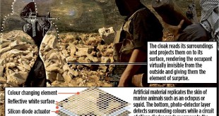
Metamaterials are artificially structured materials designed to control and manipulate physical phenomena such as light and other electromagnetic waves, sound waves and seismic waves in unconventional ways, resulting in exotic behavior that’s not found in nature. This class of micro- and nano-structured artificial media are predicted to be able to protect the building from earthquakes by bending seismic waves around it. Similarly, tsunami waves could be bent around towns, and sound waves could be bent around a room to make it soundproof.
Metasurfaces are the two-dimensional version of metamaterials: extremely thin surfaces made up of numerous subwavelength optical nanoantennas, each designed to serve a specific function upon the interaction with light. The metasurface elements act as subwavelength phase or amplitude modulators, which can be static or dynamic. Arrays of these elements act in transmission or reflection to encode arbitrary optical functionality such as focusing, steering, and other kinds of wavefront manipulation.
The main advantages of metasurfaces with respect to the existing conventional technology include their low cost, low level of absorption in comparison with bulky metamaterials, and easy integration due to their thin profile. Part of the promise of these devices lies in their ability to perform these complex optical functions using metasurfaces that are manufactured using standard lithographic techniques common in the semiconductor industry.
Optical metasurfaces have raised immense expectations as cheaper and lighter alternatives to bulk optical components. In recent years, novel components combining multiple optical functions have been proposed pushing further the level of requirement on the manufacturing precision of these objects.
Metasurfaces are an attractive alternative to conventional bulk optical components which offer the possibility to integrate complex optical functions in lightweight and cheap miniaturized components9. They hold great promise for applications such as portable or wearable devices, automotive, aeronautical and space applications and augmented/virtual reality.
Designing and fabricating optical metasurfaces requires to carefully assess the level of precision that needs to be reached to warrant the realization of the desired optical functionality with good efficiency. The discrepancies between the predicted and measured performance of metasurfaces are generally ascribed to fabrication imperfections but the relative importance of the different factors influencing their optical response is not systematically discussed.
Scientists from EPFL have developed a simple way to produce metasurfaces in just a few minutes at low temperatures, reported in Feb 2019
The production method of metasurfaces conventionally is lithography, that is a fastidious, several-hour-long process that must be done in a clean room. Now engineers from EFPL’s Laboratory of Photonic Materials and Fiber Devices (FIMAP) have developed a simple method for making them in just a few minutes at low temperatures – or even at room temperature – with no need for a clean room. The EPFL’s School of Engineering method produces dielectric glass metasurfaces that can be either rigid or flexible. The work has just been described in Nature Nanotechnology.
The new method employs a natural process already used in fluid mechanics: dewetting. This occurs when a thin film of material is deposited on a substrate and then heated. The heat causes the film to retract and break apart into tiny nanoparticles. “Dewetting is seen as a problem in manufacturing – but we decided to use it to our advantage,” says Fabien Sorin, the study’s lead author and the head of FIMAP.
With their method, the engineers were able to create dielectric glass metasurfaces – rather than metallic metasurfaces – for the first time. The advantage of dielectric metasurfaces is that they absorb very little light and have a high refractive index, making it possible to effectively modulate the light that propagates through them.
To construct these metasurfaces, the engineers first created a substrate textured with the desired architecture. Then they deposited a material – in this case, chalcogenide glass – in thin films just tens of nanometers thick. The substrate was subsequently heated for a couple of minutes until the glass became more fluid and nanoparticles began to form in the sizes and positions dictated by the substrate texture.
The engineers’ method is so efficient that it can produce highly sophisticated metasurfaces with several levels of nanoparticles or with arrays of nanoparticles spaced 10 nm apart. That makes the metasurfaces highly sensitive to changes in ambient conditions – such as to detect the presence of even very low concentrations of bioparticles.
“This is the first time dewetting has been used to create glass metasurfaces. The advantage is that our metasurfaces are smooth and regular, and can be easily produced on large surfaces and flexible substrates,” commented Sorin.
 International Defense Security & Technology Your trusted Source for News, Research and Analysis

