 International Defense Security & Technology Your trusted Source for News, Research and Analysis
Electronics are deeply embedded into the fabric of our society, changing the way we live, work and play while bringing new efficiencies to our global lifestyles, industries, and businesses. We are in the era of the digital economy and ubiquitous connectivity, and the market forces driving data and systems growth include Migration of data, logic, and applications to the cloud. Microelectronics revolution has been foundation to the advancements of these technologies.
Modern warfare is increasingly dependent on microelectronics capabilities that sense the environment, convert the signals into data streams, process the information, and generate a response. Aerospace and Defense (A-D) systems are quite similar to commercial systems that perform communications and computations, while taking advantage of the advancement of semiconductor density, functionality, and cost reduction due to Moore’s Law.
Since the 1970’s, Moore’s Law has predicted the continued increase in semiconductor areal density with a corresponding reduction in voltage, increase in switching speed, and decrease in costs. However, Moore’s Law economics are coming to an end and some key performance metrics at advanced nodes are plateauing.
On the other hand, there is the ever increased demand for more data throughput through wired and wireless systems. Cellular systems have migrated from 3G to 4G and now 5G architectures which improves bandwidth ~10X with each generation. Operationalizing of 5G communications together with Internet of Things (IoT) to Internet of Everything, Artificial Intelligence (AI) with Virtual Reality (VR) and Augmented Reality (AR), and Autonomous vehicles.
Next-generation platforms increasingly require innovative solutions that provide significantly higher performance, lower power, and smaller form factors. The explosion in data center capabilities and proliferation of IoT technologies are emerging as key drivers. In addition, advancements in terabit networking, optical transport, 8K video, and 5G wireless domains are ramping up rapidly, pushing the semiconductor industry to find innovative solutions.
Today’s demand for efficient microelectronics requires integration of materials, structures, and architectures together – not just transistor scaling, according to Dr. Michael C. Mayberry, chief technology officer at Intel. Mayberry spoke about the importance of continuing Moore’s law to advance the semiconductor industry during a Technical Leadership Panel with other semiconductor industry leaders from Texas Instruments, Raytheon Intelligence & Space, Qorvo, and SEMI Americas at the ERI Summit.
In the world of semiconductors and microelectronics, a trend to vertically stack integrated circuits (ICs) or circuitry has emerged as a viable solution for meeting electronic device requirements such as higher performance, increased functionality, lower power consumption, and a smaller footprint. The various methods and processes used to achieve this are called 3D integration technologies.
Heterogeneous Integration requirements
The market drivers for 3D heterogeneous integration range from tablets, smartphones and gaming devices to high-end computing, servers and data centers, military and aerospace, and medical devices, because they have the greatest need and can bear the cost of current 3D integration technologies. are also driving the technology.
The new Heterogeneous Integration Roadmap (HIR) provides a long-term vision for the electronics industry, identifying difficult future challenges and potential solutions. Under the sponsorship of SEMI, ASME, and three IEEE Societies, the roadmap offers professionals, industry, academia, and research institutes a comprehensive view of the landscape and strategic technology requirements for the electronics industry’s evolution over the next 15 years, and provides a 25-year vision for the heterogeneous integration of emerging devices and emerging materials with longer research and development timelines. The purpose is to stimulate precompetitive collaboration and thereby
accelerate the pace of progress
A key driving market for HI is the smartphone because of its requirement for a thin profile, low power consumption, and a drive for lower costs. This heterogeneous modularity allows for upgrading various internal devices (such as incorporating a main processor from the next node) while continuing to integrate other devices from an earlier node (such as memory).
5G Communications
Fifth-generation mobile communications (5G) represents new opportunities for IC packaging technology that are significantly different from previous generations of cellular based mobile wireless technologies. The primary focus is for millimeter-wave 5G bands, which provide the greatest challenge to packaging of RF circuits and the necessary antennas. Addressed are both base-station equipment and user equipment (UE – eg, cellphones and autonomous vehicles).
To achieve millimeter-wave high bandwidth connectivity, 5G systems will utilize beamforming technologies. Instead of wide-angle radiation patterns, narrow-focused beams will be used to track the UE devices as they move around within the operating radius of the cell site. This kind of phased-array technology has been used previously in radar systems for tracking targets. Now with 5G, phased-array beamformers will be used at higher powers at the base-station and at lower power levels at the UE.
There are three variants of beamforming: analog, digital and hybrid. Analog beamforming uses analog techniques to alter the amplitude and phase of the signal leaving each radiating element. Analog beamforming is simpler and more power-efficient as compared to digital beamforming. Digital beamforming is able to support multiple simultaneous beams but requires more power consumption due to analog-to digital conversion needed at each element. The hybrid architecture is well suited for large arrays and has perhaps the optimum architecture for massive MIMO (256 elements or more). Challenges include the small element-to-element spacing needed for the phased-array; choosing the right semiconductor technology based on the needed output power; and the integration level, multiple-band coverage, and packaging required.
IoT
The Internet of things generates demand for faster connectivity and expanded sensor capability. To meet the required performances, multiple chips are integrated into one package, together with optics (sensors) and photonics (interconnects). The increasing heterogeneity of components results in higher complexity, and eventually the package itself becomes an integral part of the system: its mechanical, electromagnetic and thermal behaviors have an impact on the overall system’s performance, reliability and cost.
Autonomous and vehicular Technology
Sensing technologies are key elements to enable migration to autonomous vehicles. The broad categories of sensors in autonomous vehicles include cameras, RADAR, LiDAR, and ultrasonics. Combinations of various sensors are needed for the fully autonomous vehicle. Cameras provide vision, but not completely. RADAR, LiDAR and ultrasonics are also essential for enabling autonomous driving. Autonomous
driving demands highly robust sensing technologies all around the car for real-time detection, surround-view, and collision avoidance. By integrating the information obtained from all these sensor systems and processing the data in real time, through machine learning and artificial intelligence, fully self-driven autonomous vehicles can be realized.
Aerospace and Defense
Several characteristics of the A-D sector create unique challenges, They are high performance so require access to leading silicon nodes and advanced packaging technologies to maintain advantage in specific technical metrics (e.g., digitization over wide bandwidths and at high dynamic range. They require High Reliability as they need to survive in harsh environments, prioritize human safety in high-risk environment. They require Long Product Lifecycles therefore managing parts obsolescence and upgradability is important. Compared to commercial sector they are Low Volumes hence require access to supply chain that provides high product mix, and business models where
NRE is managed without high volumes for amortization. Finally Security is paramount and hence require secure domestic supply chain and/or verification technologies.
Military
DoD systems for communications, radar, and sensing generally require wider bandwidths, higher dynamic range, and higher transmit power, as well as specialized frequency bands and security requirements that the commercial side does not require. To perform increasingly diverse missions in increasingly crowded EM environments, future sensor and communication systems will require increased bandwidth and sensitivity and enhanced functionality per unit area. These needs are driving sensor arrays toward 3D solutions, particularly at millimeter wave and THz frequencies
Heterogeneous integration is a factor in all of these challenges, whether by adding new twists to the challenges with multiple device technologies or by solving some of them with modular designs and assemblies. Most specifically, heterogeneous integration directly addresses the high-performance challenge for the A-D sector.
Heterogeneous Integration technology
Heterogeneous integration refers to the integration of separately manufactured components into a higher-level assembly (System in Package – SiP) that, in the aggregate, provides enhanced functionality and improved operating characteristics. In this definition, components should be taken to mean any unit, whether individual die, MEMS device, passive component or assembled package or subsystem such as high bandwidth memory (HBM), that are integrated into a single package.
Heterogeneous integration follows naturally from the conceptual vision of building large, complex systems out of smaller functions separately manufactured and packaged. Heterogeneity and the associated integration are far-reaching and can relate to materials, component types, circuit types, semiconductor nodes, interconnect methods, and source or origin.

Integration density of transistors is becoming constrained at 2D, mainly due to the slowdown in gate length shrinkage, while 3D is being utilized to continue advancement. Stacked memory as a 3D chip is an example, where multiple layers of the same technology are stacked, increasing the integration density.
Yield issues, device limitations and escalating design costs make it uneconomical to maintain the die size with technology scaling. Consequently, even though circuit elements are still scaling, performance scaling is no longer happening following Moore’s Law. Heterogeneous integration offers a solution for performance scaling. Instead of fabricating a single large multicore CPU die, smaller dies can be tiled within a package on an interposer with very short connections between the dies to realize the same performance offered by a single large die. The smaller dies have higher yields and as long as integration cost is reasonable, the overall SiP solution scales in performance following Moore’s Law.
This solution combines the right mix of functionality on the right process nodes to provide system functionality in a single package. The heterogeneous 3D SiP technology enables in-package integration of a range of components such as analog, memory, ASIC, and CPU. It also integrates transceiver die or tiles from different process nodes in the same package. New packaging technologies have enabled integrating chiplets from different manufacturing process flows into a single package with a variety of functions. The diversity of these packaging technologies has increased greatly in the past two decades, driven by market demand for higher device performance at lower cost.
Power, performance, area, and cost (PPAC) have been the key drivers for the adoption of the heterogeneous integration technology. Heterogeneous integration 3D system-in-package (SiP) technology enables next-generation platforms by offering higher bandwidth, lower latency, higher speed, lower power, a smaller form factor, and increased functionality and flexibility.
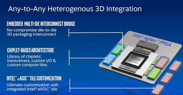
There are many examples of heterogeneous integration today, where a full subsystem or system cannot yet be fully integrated into a single semiconductor device (system-on-chip: SOC). Examples include the Intel Agilex and the AMD EPYC applications . This direction is also evident in DARPA’s CHIPS program
In general, 3D integration is a broad term that includes such technologies as 3D wafer-level packaging; 2.5D and 3D interposer-based integration; 3D stacked ICs (3D-SICs), monolithic 3D ICs; 3D heterogeneous integration; and 3D systems integration.
3D IC is an integrated circuit manufactured by stacking silicon wafers or dies and interconnecting them vertically using, for instance, through-silicon vias (TSVs) or Cu-Cu connections, so that they behave as a single device to achieve performance improvements at reduced power and smaller footprint than conventional two-dimensional processes.
3D IC is just one of a host of 3D integration schemes that exploit the z-direction to achieve electrical performance benefits. 3D IC technology finds its applications in various end-use sectors such as consumer electronics, military, information and communication technology, automotive and aerospace among others. IC manufacturers use different fabrication process for 3D ICs, depending upon requirements of the circuit system such as beam re-crystallization, wafer bonding, silicon epitaxial growth and solid phase crystallization.
3D packaging refers to 3D integration schemes that rely on traditional methods of interconnect at the package level such as wire bonding and flip chip to achieve vertical stacks. Examples of 3D packages include package-on-package (PoP) where individual die are packaged, and the packages are stacked and interconnected with wire bonds or flip chip processes; and 3D wafer-level packaging (3D WLP) that uses redistribution layers (RDL) and bumping processes to form interconnects.
2.5D interposer is a configuration where dies are mounted side-by-side on a silicon, glass, or organic interposer using through silicon vias (TSVs) through the interposer. Through silicon vias (TSVs) are holes created in a silicon wafer using an etch process. Interconnects are formed by filling TSVs with a conductive material, such as copper, tungsten, or polysilicon.
Rather than stacking wafers or die to create 3D ICs, monolithic 3D ICs begin with a base wafer onto which additional layers of crystallized silicon, metalized layers and active as well as passive circuitry are added using traditional fab equipment.
As heterogeneity increases, convergence of device, package, and PCB will increase, creating a multitude of advanced packaging solutions that have evolved to cater to specific systems. For example, high performance computing (HPC) applications demand 2.5D interposer technologies for fine pitch micro-bumping and redistribution layers (RDL). In contrast, consumer mobile and IoT markets require less stringent design rules that do not incorporate an expensive interposer, choosing to embed interconnect layers in associated mold compound using high density fan out (HD-FO) packaging technology. Interposer (TSV) and fan-out (TSV-less) technologies are not mutually exclusive and can be combined in a single, mixed technology package. The end use case largely determines the package requirement, and therefore, defines the complexity of both the device and the package.
Photonics will soon play a significant role in both enabling the use of high-end SiPs for HPC and data centers into the rest of the system as package IO solution in the near term, and ultimately to facilitate tighter integration in high-end SiPs in the longer term. The limitations of copper as an interconnection material will be addressed for SiPs for these applications, where low interconnection latency is important.
The RC delays of copper can no longer be ignored as nodes shrink below 3nm. Solutions to stretch the use of copper connections include annealing, use of shielding materials, and other approaches.
Three-dimensional circuits can be smaller, lighter and more efficient than other circuits, and 3D printing allows them to be made into arbitrary shapes that can be integrated into any object or surface.
Intel demonstrated its 3-D packaging technology in 2018
In Dec 2018, Intel demonstrated its new 3-D packaging technology, called Foveros, which allows it to stack logic chips atop one another. Various methods of going vertical have boosted memory chips recently, but after years of research, Intel will be the first to bring 3-D stacking to CPU, graphics, and AI processors at scale.
The significance of stacking extends beyond simply saving space, although that’s certainly a big part of it. It also allows you to customize combinations of silicon to your specific needs. “You can pack more transistors in a given space,” says Raja Koduri, Intel’s chief architect. “And also you can pack different kinds of transistors; if you want to put a 5G radio right on top of a CPU, solving the stacking problem would be great, because you have all of your functionality but also a small form factor.”
The first Foveros product will combine a high-performance 10nm compute-stacked chiplet with a low-power 22FFL base die. It will enable the combination of world-class performance and power efficiency in a small form factor and it also enables the combination of world-class performance and power efficiency in a small form factor.
“It’s changing the concept of the architecture,” says Maribel Lopez, founder of Lopez Research, a technology research firm. That change comes with practical benefits. The 2-D approach allows for some variety, but also sacrifices performance and draws more power, says Patrick Moorhead, CEO of Moor Insights & Strategy. Intel appears to have dodged those issues. “What is so astonishing about what has been presented is there’s virtually no power loss and no performance loss when you’re putting these chiplets together,” says Moorhead, who cautions that Intel still needs to prove that it can produce the same results across millions of chips, versus a single demonstration.
In the current scenario, two classes of chip designs are being used which is Graphics Processing Unit (GPU) and Field Programmable Gate Array(FPGA). GPU has been portraying a very crucial role in the field of deep learning such as Convolution Neural Network (CNN), Recurrent Neural Network (RNN), etc. While the reprogramming feature of FPGA makes it more usable in the machine learning industry. The chipsets are thus helping the organisations to get impact on more machine learning technologies.
World’s First 3D Printed Volumetric Circuit Emerges from University of Texas El Paso Lab
“This is a very significant step and potentially disruptive achievement,” Rumpf said. “There are many other large research groups that have been chasing this. It’s what everybody in this field is working toward and talking about, yet nobody has yet achieved it. It’s sort of the holy grail for 3-D printed circuits, and it was accomplished here at UTEP.”
Research on the 3-D/volumetric circuit technology was borne out of the notion that a three-dimensional circuit offers more freedom to make circuits smaller, lighter and more efficient. 3-D printing allows them to be manufactured into arbitrary form factors that can be integrated into any object or surface. The concept offers many opportunities for the manufacturing industry. Rumpf said this recent breakthrough came as a result of years of research and assembling all of the tools and processes it would take to accomplish.
“The last three years were spent developing futuristic CAD (computer-aided design) tools, to produce 3-D/volumetric circuits. These tools do not exist anywhere else,” Rumpf said. “I built a custom tool that allows us to place electric components in any position and in any orientation,” Carranza said. “We can route the electrical interconnects throughout all three dimensions following smooth paths.” Carranza used an open-sourced CAD software to integrate his custom functions that allowed the EM Lab to design true 3-D circuits.
“We can make circuits in any form or fashion,” Rumpf said. “You could put circuits in munitions, in eyeglasses, in shoes, and even in coffee mugs. You can be at a restaurant drinking coffee and, when the liquid gets down to a certain level the server gets notified before you have to say anything. It’s about making electronics ubiquitous in many different things.” He added that another aspect of this innovation will be the ability for small businesses that can buy a 3-D printer to become electronics manufacturers with the ability to produce products where each is customized.
“In the future, I don’t think you will see places, such as major electronics manufacturing companies, churning out billions of things and dominating the market nearly as often,” Rumpf said. “Instead, you may have thousands of small businesses in the U.S. churning out thousands of products, both mass-produced and customized. Our 3-D circuit technology may be the first step to change the paradigm of circuit manufacturing. And it may enable us to exploit and incorporate new physics in traditional planar (2-D) circuitry.
An EU-funded project developing advanced packaging for photonics, optics and electronics for low-cost manufacturing.
European Union has launched the Advanced packaging for photonics, optics and electronics for low cost manufacturing in Europe (Applause) project to rejuvenate the manufacturing and packaging value chain in Europe.
Coordinated by ICOS Vision Systems, the Applause project has 31 partners from 11 countries, including 12 large enterprises, 11 SMEs and 8 research and technology organisations (RTOs). The €34 million (approximately US$37.4 million) total budget is co-funded by the European Union’s Horizon 2020 research and innovation program as well as national funding agencies and industries in Belgium, Germany, Netherlands, Finland, Austria, France, Hungary, Latvia, Norway, Switzerland, and Israel, as a part of the Electronics Components and Systems for European Leadership joint undertaking.
The Applause project focuses on advanced packaging and assembly technologies for combined electronics, optics and photonics. The consortium members will develop new methods, processes and tools with one objective in mind: high-volume and low-cost manufacturability.
This three-year project demonstrates Europe’s ambition to be at the forefront of sensor research and technology development. Its results aim to enable more cost efficient and smaller sensors and photonics interconnects, said Stoerring. “Europe is doing well in sensors. A lot of MEMS such as accelerometers, gyroscopes, light/camera, pressure and RF MEMS, are designed and manufactured in Europe.”
Within the key technological building blocks, the consortium will work on ultra-thin wafer and die handling and packaging solutions, high-precision photonic packaging, bonding technologies for sensitive optics components, medical and biocompatible photonic packaging, as well as molding and 3D integration for optical component manufacturing. Also on the agenda is the development of test concepts and test equipment platforms and failure analysis to combine the reduced device size and the tightening alignment specifications. Members will also work on proof of high-volume, low-cost manufacturing capabilities for optics and define metrology methods and tools for advanced packaging.
The technologies will be piloted in six industrial use cases, which utilize the technology building blocks and take them toward manufacturability. The first use case, led by Austria-based AMS AG, is a substantially smaller 3D integrated ambient light sensor for mobile and wearable applications. The second one, led by Integrated Detector Electronics AS, is a high-performance, low-cost, uncooled thermal IR sensor for automotive and surveillance applications. For the third use case, Israel-based DustPhotonics Ltd. will be in charge of developing high speed datacom transceivers with reduced manufacturing costs. Datacom transceivers are used to receive and transmit signals, noted Stoerring. “Optical fibers need to be aligned to a laser die out, and this alignment is usually done actively. Here, this should be done passively, which would make the production process much easier and faster.”
On the medical front, Precordior OY and Cardiaccs AS are respectively leading uses cases for the development of a flexible patch for cardiac monitoring and miniaturized invasive cardiac sensors. Led by Finnish Vaisala OYJ, the third use case targets optical humidity measurement modules with cost-effective packaging of components.
“The developments, ongoing here, are not basic research, but they are oriented towards products,” said Stoerring. “There are several risks in this work, therefore it is difficult to say how far from commercialization the use cases will be.” He, however, noted that the flexible patch for cardiac monitoring “could come close to commercialization,” while the miniaturized invasive cardiac sensors “would probably need a lot of medical testing, and that takes time.” The optical humidity measurement modules will also need “a lot of testing afterwards”. And, because “the mobile market goes so fast, the 3D integrated ambient light sensor for mobile and wearable applications, shouldn’t be too long from commercialization.”
Because there is no technology without measurements, no quality without testing, RoodMicrotec GmbH will lead the “Testing, Reliability, Failure Analysis & Metrology” work package. And while KLA Tencor will supply inspection metrology equipment, EV Group will work on wafer-to-wafer bonding “so when we have two wafers, they can put them very well-aligned on top of each other.”
DARPA 3DSoC Program
DARPA has also launched the Three Dimensional Monolithic System-on-a-Chip (3DSoC) program focuses on developing materials, design tools, and fabrication techniques for building microsystems on a single substrate with a third upward dimension, compared to the usual flat, two-dimensional format for microelectronic chips. A primary payoff of this program could be more efficient packing of logic, memory, and input/output (I/O) elements in ways that dramatically shorten—more than 50-fold—computation times while using less power.
A pervasive challenge in leading-edge electronic systems is the time and power required for communication between processors and memory. This “memory bottleneck” it often the primary limit on system performance. Heterogeneous integration begins to address this by enabling closer integration of processor and memory devices, and DARPA recently initiated the Three Dimensional Monolithic System-on-a-Chip (3DSoC) program to further develop the technology required to build logic, memory, and input/output (I/O) on a single die. This approach will leverage established lithography nodes but improve performance via 3D integration
3D IC Market
The global market for 3D IC and 2.5D IC Packaging estimated at US$80.9 Billion in the year 2020, is anticipated to reach a revised size of US$715 Billion by 2027, growing at a CAGR of 33.50% over the analysis period 2021-2027.
Some of the semiconductor device key players are shifting their focus from analog, discrete, and logic devices to memory devices like 3D NAND and dynamic random access memory (DRAM). These factors are expected to grow the potential of the semiconductor memory devices and drive the global 3d IC market. The adoption rate of memory devices is growing owing to they are more resistive to the vibration of the devices, and the probability of data loss is comparatively less.
The demand for semiconductor devices like sensors, memory ICs, processors ICs, and the radio frequency integrated circuit has grown-up considerably from the last few years. Additionally, some of the prominent key players of smart electronics have started incorporating 3D packaging technology into their devices. The appearance of the 3D packaging technology has empowered key players to assimilate more functionalities into a single chip at a moderate price.
The memory segment is estimated to hold a dominant position in the Global 3D IC Market. The dominant position of the memory segment in the global 3D IC market can be attributed to the increasing demand for 3D memory modules. The market is beholding an increase in demand for fast, economical, and highly mountable memory module solutions across the globe.
In the consumer electronics sector the increasing number of portable devices like tablets, smartphones, or laptops are some of the major factors behind the growth of the global 3D IC market. Increasing the need for 3D ICs in sectors like servers & data hubs and the military & aerospace sector along with growing high-end computing market is also enhancing the development of the 3D IC market.
The Asia Pacific region is projected to be the leading region in the Global 3D IC Market. The leading position in the market is attributed to the presence of the end-user industries and some of the prominent key players in the region. This makes the integration of 3D IC and 2.5D IC packaging technology in the APAC region much easier. The growing demand for ICs from several end-user industries like automotive and consumer electronics, particularly for smartphones and tablets are some of the driving factors behind the growth in this region.
Furthermore, The North America region is expected to hold a significant share in the Global 3D IC Market. An increase in demand for integrated circuits in conjunction with technological upgradations is expected to drive the expansion of the 3D IC market during the forecast period.
Top Leading Companies of Global 3D IC & 2.5D IC Packaging Market are – Intel Corporation, Toshiba Corp, Samsung Electronics, Stmicroelectronics, Taiwan Semiconductor Manufacturing, Amkor Technology, United Microelectronics, Broadcom, ASE Group, Pure Storage, Advanced Semiconductor Engineering, and others.
References and Resources also include:
https://www.edn.com/heterogeneous-integration-and-the-evolution-of-ic-packaging/