 International Defense Security & Technology Your trusted Source for News, Research and Analysis
Related Articles

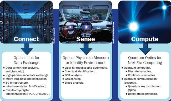
There is virtually no part of a modern defense system that is not impacted in some way by optics and photonics, even when the system is not optically based. Modern defense systems are migrating toward optically based imaging, remote sensing, communications, and weapons.
Silicon photonics uses photons to detect process and transmit information more efficiently than electrical signals, and yet have low manufacturing costs as a result of using conventional silicon-integrated-circuit processes. The same processes that have made transistors, microchips, and integrated circuits from silicon to be small, affordable, and energy-efficient devices that could execute complex tasks.
Silicon photonics has emerged as a disruptive technology to address data bottlenecks inside of systems and between computing components, enhancing power efficiency, improving response times and delivering faster insights from Big Data. Silicon photonics uses photons to detect process and transmit information more efficiently than electrical signals, and yet have low manufacturing costs as a result of using conventional silicon-integrated-circuit processes.
The demand for silicon photonics technology has increased due to their various functionalities and day-to-day use in data communication and telecommunication applications for high-bandwidth data transmission in small and long networks. Active optical cables in these applications can provide a high-speed data transmission rate of digital information in data centers and networking communication, the release said.
Also, it fulfills the need for data transfer rate for cloud-based services in the corporate sector.The demand for high-speed data transfer in data centers is expected to boost the market for silicon photonics technology. In this application, silicon photonics enhances performance in terms of computation, communication, and measurement to fulfill the needs of consumers and enterprise cloud services.
Silicon Photonics shall also benefit other application areas such as fibre-to-the-home (FTTH) or fibre-to-the-premises (FTTP), environmental monitoring, biological and chemical sensing, microwave photonic circuits, medical and military applications and astronomy. Eventually, the technology could reach home computers and mobile devices and improve applications from gaming to video streaming.
The Silicon Photonics Applications Space. Courtesy of SOITEC.
Military and Aerospace Applications
PICs are devices analogous to electronic integrated circuits but use light rather than electrons for information signaling and transfer. While electronic integrated circuits are usually constructed as arrays of transistors, PICs employ a range of components (e.g., waveguides) to focus, split, isolate, polarize, couple, modulate, and, ultimately, detect light. Technical advancements in materials fabrication—realized especially over the past two decades—have enabled embedding these numerous functions in a single small-footprint PIC device. PICs are increasingly applied in telecommunications and sensing platforms.
When it comes to spacecraft, planes and military gear, weight is all important. That’s understandable, as it costs about $10,000 to put a pound in orbit, in the case of spacecraft. For planes and military gear, there are limits on what can be flown or carried. Hence, the importance of keeping weight down — and the growing interest in and use of photonic integrated circuits (PICs). “We’re buying size, weight and power,” said Michael Krainak head of the laser and electro-optics branch at NASA Goddard Space Flight Center in Greenbelt.
In an October 2016 presentation, Krainak said that the areas where photonics could help aerospace include sensing and communications. Defense application areas are the same, although military uses will also likely include remote detection of chemical and biological agents as well as explosives, Krainak added in a later conversation
Other promising applications include optical gyroscopes that are widely used in vehicle navigation. They use laser beams in a fibre-optic loop, and the beams produce interference when the device’s orientation changes. Optical devices are more accurate than their mechanical counterparts, but are hard to miniaturize. Andrey Matsko and his colleagues at OEwaves in Pasadena, California, have made one with a volume of just 15 cubic centimetres. Instead of producing interference in a large fibre-optic loop, the light resonates inside a minuscule crystalline cavity. The gyroscope drifts by only three degrees per hour, an order of magnitude better than previous efforts. Other sensing applications could involve optical accelerometers and multiwavelength imagers.
Vehicle health monitoring applications are also important because airplanes, spacecraft and military vehicles are subject to repeated and sometimes violent movement, which causes strain. This can be measured by writing a Bragg grating into an optical fiber and then attaching the fiber to the component of interest.
“A fiber Bragg grating reflects one part of the light. If you stretch this grating, you will get a slight change of the reflected light. That is what we are looking at and basically you do that with a narrow band spectrometer,” said Pim Kat, president and CEO of the Technobis Group. Located in Alkmaar, the Netherlands, the company concentrates on aerospace and medical applications.
In the past, this measurement has been done using free space optics, which leads to large, heavy, expensive and power-hungry systems, as compared to what’s possible with photonic integrated circuits. Richard Visser is CEO of Smart Photonics BV, an Eindhoven, Netherlands-based foundry that works exclusively in indium phosphide. He said that the integrated strain-measuring chips are only a few square millimeters in size, making them much smaller and lighter than the free space optics equivalent. “They are also thousands of times more accurate due to a lack of vibration effects,” Visser said.
Because of these characteristics, systems built using integrated components can be deployed in more places aboard a vehicle. This means its health can be more closely monitored, which is of interest to both civilian and military aircraft makers and users
Lidars
Lidars (Light Detection and Ranging) are similar to radars in that they operate by sending light pulses to the targets and calculate distances by measuring the received time. LIDARs are rapidly gaining maturity as very capable sensors for number of applications such as imaging through clouds, vegetation and camouflage, 3D mapping and terrain visualization, meteorology, navigation and obstacle avoidance for robotics as well as weapon guidance.
“It is useful in missile guidance and tracking, autonomous flight, and aircraft damage detection. Implementing this technology using photonic integrated circuits would cut size and cost,” said Jose Pozo, director of technology and innovation at the European Photonics Industry Consortium,
Lidars are costly and bulky instruments which make their integration in a car challenging. Within a promising ADAS market silicon photonic based lidar will play a key role. Indeed silicon photonics allow lidar without moving elements, which can experience issues in a harsh car environment . Last august, MIT’s Photonic Microsystems Group announced a successful DARPA project using silicon photonics for lidar on a chip with steerable transmitting and receiving phased arrays and on chip Ge photodetectors.
Silicon Photonics for Space Communications
Space optical communications is an emerging area of research not just for NASA and large agencies but also small-business micro/nano-satellite companies. The Wavelength division multiplexing or coherent communications requires many lasers, which are inefficient and potential failure points. Mode-locked lasers are complex and expensive to stabilize. High-efficiency, high-bandwidth laser arrays have proved difficult to realize, and the state-of-the-art in heterogeneously-bonded lasers is very expensive, and temperature-sensitive, says NASA.
Xiaoxi Wang, University of California, San Diego is designing a photonic transmitter microchip at 1.550 um wavelengths (the NASA-chosen wavelength for near-earth laser comm.) which can scale to 200 Gbit/s and beyond, with silicon photonic coherent optical communications. Off the-shelf single-laser optical transmitters used in current micro-satellites operate only up to 200 Mbit/s.
“To increase bit rate by such a large factor, we need to encode information on multiple carriers. I am developing a novel integrated photonic architecture in which an integrated recirculating frequency shifter (RFS) generates multiple carrier tones from only one seed laser diode. The proposed research is to design a monolithic silicon photonic chip in which the seed laser is modulated by a single-sideband modulator and is fed back in a loop through tunable optical bandpass filters and gain to generate a controllable number of “teeth” in a frequency comb.”
Biosensing
The Department of Defense (DoD) has broad needs to deploy better biochemical sensors for applications in medical diagnostics, environmental monitoring, rapid identification of threats, hazardous materials control, basic scientific research, and more. For example, point-of-care detection of biomarkers of injury or disease can provide rapid health status assessments and quicker medical responses in the field. Standoff detection of chemical and biological threats, such as nerve agents and bioweapons, using long-range sensors is an integral component of force protection strategies as weapons proliferate. Urban environment operations also require monitoring for toxic industrial chemicals and materials to ensure the health and safety of service members. Biochemical sensors capable of tackling these DoD challenges must detect specific molecules within complex mixtures at high confidence; they must also be relatively inexpensive, easy to operate, and sufficiently robust for operational field use. To this end, optical-based sensing using photonic integrated circuits (PICs) has emerged as a promising technology.
DOD initiative for Integrated photonic circuits
DoD officials cited the following as impacts enabled by integrated photonics:
— Next-generation information processing, communications and data storage enabled by integrated photonics will lower the costs of broadband access and the efficiency of long-haul, metropolitan and local-area networks.
— Integrated photonics use in green data centers will enable 100 Gb/s speeds with less power per bit than current 10 Gb/s solutions, resulting in millions of dollars per year in energy savings.
— Significant reductions in size, weight and power enabled by photonics-electronics integration will be critical for embedded computing systems for mobile platforms, image processing and remote sensing.
— Integrated photonics will enable a several-fold increase in the dynamic range of detectors, resulting in the ability to “see through” complex media such as human tissue to significantly improve detection for some diseases.
— Advances in integrated photonics will lead to significant improvements in the ability to see through dust clouds of landing helicopters, avoiding crash landings and saving warfighter lives.
Integrated Photonics Institute for Manufacturing Innovation (IP-IMI)
The U.S. Government has awarded to a multi-partner consortium led by the State University of New York (SUNY) of a $110 million matching grant to establish an Integrated Photonics Institute for Manufacturing Innovation (IP-IMI), the sixth Institute for Manufacturing Innovation.
It is intended to advance the state of the art in the design, manufacture, testing, assembly, and packaging of complex photonic integrated circuits that combine a variety of photonic and electronic components to achieve functionality.
The proposal noted that integrated photonics manufacturing has the potential to revolutionize the carrying capacity of internet networks to transmit more data at faster speeds; enhance medical technology; reduce the cost of sequencing the human genome; and improve battlefield imaging and radar capabilities for national defense.
It is intended to bridge the gap between basic/early research and product development and introduction by developing and scaling critical technologies in the manufacturing readiness level 4 to 7 range.
Earlier, The U.S. Department of Defense launched initiative for ramping up of domestic manufacturing of photonic integrated circuits effort, by disbursing up to $110 million in federal funding via an Integrated Photonics Manufacturing Institute.
“For photonics technology you have a large commercial potential, a defense requirement, and a growing but fragmented industry that lacks standards and advanced manufacturing processes to be able to move from the laboratory environment to full-scale commercial applications.” said Adele Ratcliff, director of manufacturing technology in the Office of the Deputy Assistant Secretary of Defense as reported by DOD News.