 International Defense Security & Technology Your trusted Source for News, Research and Analysis
Related Articles

The goal of future generation networks is to meet the future communication needs of the information societies such as Smart infrastructures, Smart City, Smart Grid, Smart Health, and Smart Transportation. The future will be a completely data-driven society in which people and things are connected universally, almost instantaneously (milliseconds) to form an incredibly fully connected utopian world. It will also be key enabling technology to fully realize the Industry 4.0 revolution i.e., the digital transformation of manufacturing through cyber physical systems and IoT services. Wireless communication carrier frequencies have been gradually expanding over recent years in an attempt to satisfy ever-increasing bandwidth demands. The peak rate, which is one of the key technical indicators is expected to reach tens of terabits per second.
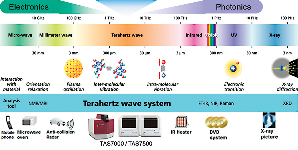
In the past, the frequency spectrum ranging from 0.3 to 3THz (or 300 to 3000GHz) was spoken as infamous “Terahertz Gap” as it lies between traditional microwave and infrared domains but remained “untouchable” via either electronic or photonic means. The conventional “transit-time-limited” electronic devices can hardly operate even at its lowest frequency; the “band-gap-limited” photonic devices on the other hand can only operate beyond its highest frequency. However continuous progress is being made for Terahertz components and devices to overcome electronic/photonic barriers for realizing highly integrated Terahertz systems.
Due to the lack of compact and efficient THz devices (the so-called “THz gap”), THz-band applications have been traditionally restricted to the areas of imaging and sensing. However, following recent advancements in THz signal generation, modulation, and radiation, communication based THz-band use cases can now be foreseen
Terahertz can provide hundredfold, increase in the frequency compared to the mmWave addressing spectrum scarcity and capacity limitation in current wireless systems. Terahertz wi-fi could in theory support data rates up to 100Gb/s within ranges of about 10m. THz ad hoc network can be formed in the battlefield to connect soldiers, armoured personnel carriers, tanks, etc. The limited transmission range and highly directional antennas makes eavesdropping extremely difficult.
“Imaging, radar, spectroscopy, and communications systems that operate in the millimeter-wave (MMW) and sub-MMW bands of the electromagnetic spectrum have been difficult to develop because of technical challenges associated with generating, detecting, processing and radiating the high-frequency signals associated with these wavelengths. To control and manipulate radiation in this especially challenging portion of the RF spectrum, new electronic devices must be developed that can operate at frequencies above one Terahertz (THz), or one trillion cycles per second,” says DARPA.

The researchers have created many breakthroughs in terahertz technologies recently that has led to testing and deployment of terahertz wireless links. The Researchers from the Tokyo Institute of Technology have already demonstrated 3Gb/s transmission at 542 GHz. At the heart of the team’s 1mm-square device is what is known as a resonant tunnelling diode, or RTD. During the 2008 Olympic Games in Beijing, scientists from Osaka University and NTT Corp. already demonstrated a 120 GHz data link across a distance of 1 km.
Nevertheless, there still exist many challenges in THz communications requiring innovative solutions, where the well-established technologies may be prohibited. Sensitive to atmospheric attenuation and molecular absorption, the THz signals experience an extremely severe path loss, which leads to a great limitation on communication distance. Meanwhile, the complex structures of THz devices pose extra constraints on the system, where conventional approaches, e.g., completely digital signal processing at baseband for each antenna, are no longer suitable.
THz Communications technologies
In the meantime, marvelous advances in hardware are making THz communications a reality. Currently, high-performance Silicon-Germanium (Si-Ge) based front-ends can generate signals up to 0.84 THz. Besides, the study on transceivers with Gallium-Nitride (GaN) based power amplifiers has demonstrated capabilities over 1 THz.
Many new compact, room temperature, terahertz sources are being developed. Teraphysics has developed miniature helical TWT for operation at 650 GHz under contracts from NASA Jet Propulsion Laboratory (JPL), the Defense Advanced Research Projects Agency (DARPA), the Army Research Office (ARO), and the Air Force Office of Scientific Research (AFOSR).
Photonic devices, such as Quantum Cascade Laser (QCL) sources, are also investigated for the THz band. Specifically, THz digital-to-analog (D/A) converters and analog-to-digital (A/D) converters have been designed using radio-frequency (RF) photonic technology.
Moreover, the magnet or voltage controlled THz phase shifters based on graphene/liquid crystal have been developed at room temperature for THz beamforming. In addition, novel nano-devices, e.g., compact graphene antennas, will be feasible for THz transmission in the near future. Undoubtedly, this ultra-broadband communication is just around the corner.
The significant decrease in the wavelength in terahertz enables packing a large number of antennas in a small area, which could provide more gains to establish reliable links. Thus, gains from multiple antennas should be explored to combat and compensate for such losses.
“We now have many enabling technologies thanks to the recent progress of semiconductor devices and integrated circuits operating at THz frequencies,” Nagatsuma of Osaka University told Nature Photonics. “In addition to the data rate, other expected advantages of THz communications over microwave communications are low power consumption and smaller transceiver size, particularly coming from a reduction in the antenna size,” he added.
THz Components
Sources
CW-sources based on microwave technology and solid state sources based on quantum cascade laser technology are now available and offer average power in the mW range. Dramatic improvements have also been made in the generation of intense picosecond THz pulses via nonlinear optical methods such as optical rectification. It is now possible to routinely generate pulse energies of tens of micro-joules and field strengths exceeding 1 MV cm−1 with a compact and reliable femtosecond laser source in a small university laboratory.
Many new compact, room temperature, terahertz sources are being developed. Led by Associate Professor Yang Hyunsoo and Dr Wu Yang from the Department of Electrical and Computer Engineering at the NUS Faculty of Engineering and NUS Nanoscience and Nanotechnology Institute, the research team has successfully developed high performance and low-power driven THz emitters that could be mass-produced at low cost, addressing a critical challenge for industrial application of THz technology. These THz emitters, which are used for the generation of THz waves, can also function on flexible surfaces without compromising on performance.
Our invention is a big step forward in THz technology and we believe that this will greatly accelerate its application in various fields. For instance, in the area of safety surveillance, our invention can contribute towards miniaturisation of bulky THz systems to be used in the detection of dangerous chemicals and explosives for protection against hostile threats. Affordable and high performance THz screening devices could also improve disease diagnosis and benefit patients. Furthermore, fabricating our device on a flexible surface also opens up many exciting possibilities for it to be incorporated into wearable devices,” explained Assoc Prof Yang.
Developed using metallic thin film heterostructures that are 12-nanometre in thickness, the novel radiation sources emit broadband THz waves with a higher power output than a standard 500-micrometre thick rigid electro-optical crystal emitter. In addition, the novel emitters can be powered by a low-power laser, hence lowering the operating cost substantially.
The research team also devised a novel, low-cost fabrication technique to produce the emitters. A large wafer-scale film can be deposited and subsequently diced to a large quantity of ready-to-use devices, thus making this production method commercially scalable. The research team also tested their device on flexible surfaces and found that its performance was not compromised despite being subjected to a large bending curvature.
Vacuum electronic devices (VEDs) convert electrical stored energy into kinetic energy of an accelerated electron beam, which is then converted into electromagnetic field energy with the aid of electromagnetic waveguides or cavities, defined as an interaction zone or circuit.Due to physical limits on power density management, VEDs present the only practical solution for high power, compact, efficient sources (oscillators, amplifiers) of 0.1–1.0 THz radiation. VED oscillators and amplifiers have been designed and operated at 0.220–1.0 THz and 10 mW–1 MW with high efficiencies (0.5–20% and above). Such performance is unachievable by any other technology. The ability to achieve exceptionally high overall efficiency by spent beam energy recovery is uniquely available to VEDs and not possible with any other compact THz radiation source.
Teraphysics has developed miniature helical TWT for operation at 650 GHz under contracts from NASA Jet Propulsion Laboratory (JPL), the Defense Advanced Research Projects Agency (DARPA), the Army Research Office (ARO), and the Air Force Office of Scientific Research (AFOSR)
Manijeh Razeghi, director of the Center for Quantum Devices in the McCormick School of Engineering and Applied Science and her team have generated terahertz radiation through nonlinear frequency mixing of two mid-infrared wavelengths at 8.8 microns and 9.8 microns from a single QCL chip.
A major source of THz radiation is the quantum cascade laser (QCL), semiconductor device that could emit high power narrowband THz radiation between 1 and 5THz, is revolutionizing the THz field. It achieves laser emission by exploiting phenomena that emerge from a repeated stack of semiconductor multiple quantum well heterostructures. QCLs have shown remarkable performances over the range 1–5 THz range, with demonstration of high powers (>1 W), photonic and far-field engineering, a quantum limited linewidth, frequency combs and pulse generation. These advances have permitted THz QCLs to be made commercially available and, although cryogenic cooling is still required, this can be achieved conveniently and inexpensively with Stirling coolers.
At room temperature, continuous terahertz emission with 3 microwatts is realized in a monolithic nonlinear QCL device with a tiny packaging dimension (as small as 2x5x8 mm3). This research was partially supported by the National Science Foundation, Department of Homeland Security, Naval Air Systems Command, and NASA.
Terahertz source breakthrough
Electrical and optical engineers in Australia have designed a novel platform that could tailor telecommunication and optical transmissions. Collaborating scientists from the University of New South Wales in Sydney and Canberra, the University of Adelaide, the University of South Australia and the Australian National University experimentally demonstrated their system using a new transmission wavelength with a higher bandwidth capacity than those currently used in wireless communication.
“I think moving into terahertz frequencies will be the future of wireless communications,” said Shaghik Atakaramians, an author on the paper. However, scientists have been unable to develop a terahertz magnetic source, a necessary step to harness the magnetic nature of light for terahertz devices.
In previous work, Atakaramians and collaborators proposed that a magnetic terahertz source could theoretically be produced when a point source is directed through a subwavelength fiber, a fiber with a smaller diameter than the radiation wavelength. In this study, they experimentally demonstrated their concept using a simple setup — directing terahertz radiation through a narrow hole adjacent to a fiber of a subwavelength diameter. The fiber was made of a glass material that supports a circulating electric field, which is crucial for magnetic induction and enhancement in terahertz radiation.
Creating terahertz magnetic sources opens up new directions for us,” Atakaramians said. Terahertz magnetic sources could help the development of micro- and nanodevices. For example, terahertz security screenings at airports could reveal hidden items and explosive materials as effectively as X-rays, but without the dangers of X-ray ionization.
Another advantage of the source-fiber platform, in this case using a magnetic terahertz source, is the proven ability to alter the enhancement of the terahertz transmissions by tweaking the system. “We could define the type of response we were getting from the system by changing the relative orientation of the source and fiber,” Atakaramians said.
Atakaramians emphasized that this ability to selectively enhance radiation isn’t limited to terahertz wavelengths. “The conceptual significance here is applicable to the entire electromagnetic spectrum and atomic radiation sources,” said Shahraam Afshar, the research director. This opens up new doors of development in a wide range of nanotechnologies and quantum technologies such as quantum signal processing
Detectors
Researchers at Chalmers University have developed a flexible detector for terahertz frequencies using graphene transistors on plastic substrates. The detector—which converts RF energy to a DC signal so the power of the signal can be measured—is the first of the kind, said Jan Stake, professor and head of the Terahertz and Millimetre Wave Laboratory in Chalmers’ Department of Microtechnology and Nanoscience.
“A detector is a key component in any high-frequency application,” he told Design News. The device can extend the use of terahertz technology to applications that will require flexible electronics, such as wireless sensor networks and wearable technology. “Graphene is a promising material for high-frequency application thanks to high carrier mobility, and mechanically strong for just a monolayer,” he said. “This combination can open up for flexible terahertz applications.”
At room temperature, the detector—which is translucent and flexible—can detect signals in the frequency range 330 to 500 gigahertz, researchers said. This technique has a number of applications, including for imaging in the terahertz area—such as in a terahertz camera–as well as for identifying different substances, such as in sensors.
New terahertz detectors are being developed which don’t require require cryogenic cooling or bulky optical equipment. The researchers from the University of Maryland have used “hot-electron photothermoelectric effect” to build a prototype detector capable of sensing terahertz waves at room temperature.
Another advance towards compact, sensitive and fast THz detectors was announced recently by Italian and French researchers. By exploiting the excitation of plasma waves in FETs, they have been able to create the first detectors based on semiconductor nanowires. The new nanowire detector operates at room temperature, can reach detection frequencies greater than 3THz, has a maximum modulation speed in the MHz range and a noise performance already competitive with the best commercial technologies, said Miriam Serena Vitiello, leader of the Terahertz Photonics Group in the Nanoscience Institute in Pisa. Vitiello says: “The aim now is to push performance into the ultrafast detection realm, explore the feasibility of single photon detection by using novel architectures and material choices, develop compact focal plane arrays, and to integrate on chip the nanowire detectors with
The research of Semiconductor Research Corporation (SRC) has showed that it is possible to manufacture circuits operating in the terahertz range using the CMOS processes at a greatly reduced cost that was possible earlier. The key to SRC success is the way to manufacture scottky diodes on CMOS using the same process. They fabricated an Image sensor, employing scottky diodes in the 130 nanometers CMOS, at 280 GHz and 860 GHz frequency with enhanced detector sensitivity.
Terahertz Multiplexers / Demultiplexers
Multiplexers / Demultiplexers are devices that are used to enable separate streams of data to travel through a single medium, by combining the signals through multiplexers at the transmitter end and separating them through demultiplexers at the receiver end, common examples are cable carrying multiple TV channels or fiber optic line carrying thousands of phone calls at the same time.
Researchers from Brown University have developed deices for multiplexing / demultiplexing terahertz waves. The multiplexer that Mittleman and his colleagues have been working on makes use of what’s known as a leaky wave antenna. In this case, the antenna is made from two metal plates placed in parallel to form a waveguide. One of the plates has a small slit in it. As terahertz waves travel down the waveguide, some of the radiation leaks out of the slit. It turns out that terahertz waves leak out different angles depending on their frequency.
“That means if you put in 10 different frequencies between the plates — each of them potentially carrying a unique data stream — they’ll come out at 10 different angles,” Mittleman said. “Now you’ve separated them and that’s demultiplexing.” On the other end, a receiver could be tuned to accept radiation at a particular angle, thus receiving data from only one stream.
“We think it’s definitely a reasonable solution to meet the needs of a terahertz communication network,” said Nicholas Karl, a graduate student at Brown and the paper’s lead author. Karl led the experiments on the device with fellow graduate student Robert McKinney. Other authors on the study are Rajind Mendis, a research professor at Brown, and Yasuaki Monnai from Keio University in Tokyo. The group plans to continue its work to refine the device. A research group from Osaka University is collaborating with Mittleman’s group to implement the device in a prototype terahertz network they’re building.
Tufts Researchers Build A Chip-Sized, High-Speed Terahertz Modulator
Tufts University engineers claim to have a breakthrough with their successful fabrication of an on-chip device that can perform gigahertz-rate amplitude modulation, and switching of broadband terahertz electromagnetic waves confined within a novel slot waveguide with tunable, two-dimensional electron gas.
“A prototype device is fabricated which shows THz intensity modulation of 96% at 0.25 THz carrier frequency with low insertion loss and device length as small as 100 microns. The demonstrated modulation cutoff frequency exceeds 14 GHz indicating potential for the high-speed modulation of terahertz waves. The entire device operates at room temperature with low drive voltage (<2 V) and zero DC power consumption,” the researchers wrote in a paper published in Scientific Reports.
Previously-built THz modulators were capable of reaching speeds of only up to a few kilohertz (kHz). The Tufts University team claims to have experimental results showing gigahertz speed modulation of THz waves for the first time.
“This is a very promising device that can operate at terahertz frequencies, is miniaturized using mainstream semiconductor foundry, and is in the same form factor as current communication devices. It’s only one building block, but it could help to start filling the THz gap,” said Sameer Sonkusale, Ph.D., of Nano Lab, Department of Electrical and Computer Engineering, Tufts University, and the paper’s corresponding author, in a news release.
A well-known application for building fast and compact terahertz modulators is to achieve high data rate wireless communication, where an inherently high carrier frequency of THz wave will support much wider signal bandwidth compared to the radio frequency (RF) bands used today, according to the researchers. But wider applications abound, such as in material identification, imaging, wireless communications, chemical and biological sensing.
THz Antenna
Due to the enormous path loss for long distance in space and tiny power capacity, the high gain antenna is preferred. The traditional reflector antenna used for THz band will bring some problems because of the extremely higher requirement of surface precision, although this kind of antenna has larger gain.
A team headed by physicists Alexander Holleitner and Reinhard Kienberger from the Technical University of Munich (TUM) has generated ultrashort electric pulses on a chip using metal antennas only a few nanometers in size. Pulses of femtosecond length from the pump laser generate on-chip electric pulses in the terahertz frequency range. With another laser, the information is read out again.
Physicists from the Technical University of Munich (TUM) exploited femotsecond photoswitches based on the nanoscale metal structures to drive the pulses. The nonlinear ultrafast response was based on a plasmonically enhanced, multiphoton absorption, resulting in a field emission of ballistic hot electrons propagating across the nanoscale structures.
According to researchers, a femtosecond laser pulse with a frequency of 200 THz could generate an ultrashort terahertz signal with a frequency of up to 10 THz in the circuits on the chip. Researchers used sapphire as the chip material because sapphire cannot be stimulated optically and would therefore cause no interference. Lasers with a 1.5-μ wavelength were used in traditional internet fiber optic cables.
THz Signal Processing
The classical signal processing method cannot fully benefit from the properties of the THz band signal. The new channel models are required for the THz wave propagation. New coding schemes are needed to overcome the channel errors in the THz band. Different bandwidths and transmission distances of THz wave applications require various adaptable modulations.
Low-cost system architectures and communication schemes are needed, which should be adaptive and stable to the whole THz band.
Terahertz Photonics
“Scientists are turning to the development of photonic, rather than electronic, devices for THz communications because it is easier to achieve higher data rates using photonic components,” said Nagatsuma of Osaka University. “In addition, photonics-based systems might be deployed in the future convergence of fibre optic and wireless communications networks,” commented Nagatsuma. He believes that ultrawideband amplifiers and antennas are the most crucial components needed to make full use of the bandwidth. “Even for photonics-based systems, amplifiers are necessary to boost the output power in the transmitter and to increase the sensitivity in the receiver,” he stressed.
“Therefore, over the past 10 years many developments have been made to prepare for the future convergence between fiber optic and mobile end users, in backhaul — point to point (P2P) — or fronthaul schemes,” writes Guillaume Ducournau, Institute of Electronics, Microelectronics and Nanotechnology. “Both require very high frequency transceivers, and electronic/optic approaches are under investigation. In addition, the massive development of multilevel encoding combined with standard WDM (wavelength division multiplexing) and the context of coherent networks and core signal processing is now established. Thus, the quest for direct optical to radio transceivers has become very attractive and would enable direct bridges between optical data rates and mobile data delivery.
THz communication devices will require innovation in integration and packaging to be practical. Guillermo Carpintero of Universidad Carlos III de Madrid in Spain described how he and his co-workers are tackling this challenge and have developed integrated photonics-based sources of millimetre and THz waves during 40th International Conference on Infrared, Millimeter, and Terahertz Waves (IRMMW-THz).
“Although we tried to use available generic integration-platform building blocks, there is no building block for Bragg mirrors,” said Carpintero. As a result, the team developed the concept of integrated multimode interference reflector mirrors for mode-locked lasers. The optical spectrum of the optical heterodyne source based on the mode-locked photonic integrated circuit around 1,560 nm showed a carrier wave frequency of 90 GHz. The team has used this on-chip optical heterodyne source to perform broadband wireless data transmission.
“For nomadic usages, development of siliconbased photonics and/or CMOS might enable advanced integration and miniaturization, which is especially required for mass market applications, such as those embedded in mobile terminals,” writes Guillaume Ducournau.
Advances in Terms of Materials
Large bandgap semiconductor materials have proven to be promising semiconductor materials for achieving THz devices with higher photon frequencies and emission powers. Among these materials, GaN and GaAs have been the most favorable materials. The bandgap energy, saturation velocity, and thermal conductivity of GaN are all more than twice that of GaAs. As a result, GaN devices offer higher output power
and operation frequency compared with other conventional III to V devices. The mentioned characteristics of GaN together with its capabilities of providing high 2-D electron densities and high longitudinal-optical (LO) phonon of ∼90 meV make it one of the most promising semiconductors for the future of generation, detection, mixing, and frequency multiplication of electromagnetic waves in the THz frequency regime.
InP Devices
To date, the terahertz band is mostly unused for a lack of suitable electronic components, which are commercially available only up to around 100 GHz.” In order to reach these high frequencies, both intrinsic and extrinsic parasitic capacitances need to be reduced, and semiconductor materials with high electron mobility need to be used. For this purpose, we developed a transfer-substrate Indium Phosphide (InP) Hetero-Bipolar Transistor technology. Besides high electron mobility, the InP material system offers a high breakdown field due to its large energy gap, enabling higher output power at THz frequencies than any other semiconductor material,” write Leibniz-Institute IHP Frankfurt. Capacitances are effectively reduced with the transfer-substrate approach.
“InP HBTs with an emitter size of 0.5 × 5 µm2 are defined by electron beam lithography, demonstrating an fmax of more than 450 GHz at a breakdown voltage of BVCEO = 4.5 V. Monolithically integrated circuits such as amplifiers, mixers, and oscillators operating in the frequency range from 100 GHz to over 300 GHz have been fabricated and tested.”
The cutoff frequency of ultra-high frequency transistors is increased with geometrical device scaling. The cooling of these transistors becomes ever more important as the power density increases with shrinking device dimensions. The heat can be efficiently extracted from the transistors with the integration of an electrically isolating diamond heat spreading layer, without having to compromise the high frequency performance. The thermal resistance of diamond-integrated InP HBT could be reduced by more than a factor of three compared to standard InP HBT, reaching a value below 1 K/mW. The RF output power of analog amplifier circuits operating at around 100 GHz could be doubled with the inclusion of the diamond heat sink.
System integration of integrated terahertz circuits requires a suitable mounting technology, foremost to connect the terahertz circuit to an antenna structure. The required mounting and connection technology needs to be sufficiently broadband, should not incur significant RF losses, must be reproducibly manufacturable from the initial electromagnetic design, and needs to be low cost. Classic bond wire connections are difficult to implement beyond 100 GHz due to manufacturing tolerances.
A flip-chip mounting technology based on gold-tin with 10 µm design rule was developed, including multilayer passive submount substrates with shielded transmission lines, which were manufactured in a process sequence similar to the InP DHBT process flow. Passive and active InP HBT circuits were mounted onto these submounts and measured. A bandwidth from DC to 450 GHz could be demonstrated. The insertion loss of the flip-chip transitions was less than 1 dB even at the highest frequencies.
Wafer-scale InP DHBT – SiGe BiCMOS hetero-integration process – SciFab
“Based on the transferred-substrate concept, we developed a wafer-scale 3D integration approach of InP DHBT technology onto Silicon Germanium Bipolar-CMOS (SiGe BiCMOS) wafers using face-to-face adhesive wafer bonding, subsequent InP substrate removal, and formation of vertical RF interconnects between the InP DHBT and SiGe BiCMOS subcircuits. In this complementary approach, we combine the advantages of both technologies: highly complex BiCMOS analog and digital circuits are augmented with the high bandwidth and output power of InP DHBT amplification and mixing stages. Signal sources including a BiCMOS VCO and InP mixing and power amplification stages operating at up to 330 GHz were demonstrated.”
Other Components
DARPA has made a series of strategic investments in terahertz electronics through its HiFIVE, SWIFT and TFAST programs.
Northrop Grumman Corporation, under DARPA’s Terahertz Electronics, has created a fastest solid-state amplifier integrated circuit ever measured, operating at a speed of one terahertz. The ten-stage common-source amplifier Terahertz Monolithic Integrated Circuit (TMIC) exhibits power gains several orders of magnitude beyond the current state of the art, using a super-scaled 25 nanometer gate-length. The Northrop Grumman TMIC showed a measured gain of nine decibels at 1.0 terahertz and 10 decibels at 1.03 terahertz.
DARPA has also demonstrated a 0.85 Terahertz power amplifier using a micromachined vacuum tube—a world’s first. The achievement comes from DARPA-funded researchers at Northrop Grumman Electronic Systems, who built the 1 centimeter-wide traveling wave vacuum tube.
Researchers of Fraunhofer Inst. for Appl. Solid State Phys. (IAF), Freiburg, Germany, have developed a compact 500-750 GHz low-noise amplifier (LNA) circuit, based on a grounded coplanar waveguide (GCPW) technology utilizing 20 nm metamorphic high electron mobility transistors (mHEMTs). The realized six-stage LNA TMIC achieved a maximum gain of 15.4 dB at 576 GHz and more than 10 dB in the frequency range from 555 to 619 GHz. University of Utah electrical and computer engineering professor Ajay Nahata, left, and U graduate student Andrew Paulsen, have designed a terahertz frequency filter made through a process they developed with an inkjet printer.
References and resources also include:
https://www.sciencedaily.com/releases/2018/02/180206115340.htm