 International Defense Security & Technology Your trusted Source for News, Research and Analysis
As copper reaches its speed limit, engineers look at optics to replace copper for very high speed signals. The electronic transmission of information requires energy – the faster the interface, the more electrical power is required. At very high data transfer rates, optical interfaces can be significantly more efficient than electrical ones. Engineers also envisage replacing copper links between servers, routers, and switches with active optical cables.
Current technological trends such as big data processing, global social-media networks, and the Internet of Things (IoT) require advanced processing structures. The rise of photonic integrated circuits and even quantum computers based on light leads to the question of how to connect these optical processing units. Already silicon chips are available with some optical components inside. For long-distance transmission, glass fibers are certainly a good solution. But for short distances, such as inside devices, this approach leads to a chaos of wiring similar to what could be found in electrical devices from the first half of the last century.
The solution for electrical wiring chaos was the introduction of printed electrical connections, later known as printed circuit boards (PCBs). The function of a electronic printed circuit board (PCB) is to mechanically support and electrically connects electrical or electronic components using conductive tracks, pads and other features etched from one or more sheet layers of copper laminated onto and/or between sheet layers of a non-conductive substrate. PCB connects a variety of active components (such as microchips and transistors) and passive components (such as capacitors and fuses) into an electronic assembly that controls a system. A typical printed circuit board consists of conductive “printed wires” attached to a rigid, insulating sheet of glass-fiber-reinforced polymer, or “board.” The insulating board is often called the substrate.
Electro-optical printed circuit boards are circuit boards with both optical and electrical layers, combining optical and copper paths on the same board. While the copper paths distribute power and low-speed data, the optical paths handle the high-speed signals. This segregation has several advantages. At high frequencies, signal integrity suffers due to skin effect, crosstalk, and skew when passing through copper systems. Optical systems do not have those issues, while also presenting greater channel density than copper does. Moreover, as optical signals do not need signal conditioning and equalization, optical systems consume lower power than do electrical signals. Additionally, optical systems can reduce the surface area of a PCB by 20% and the number of layers on the board by 50%. And of course, EOCBs need to fulfill a number of general requirements, with low cost, reliability, and easy manufacturability being most important.
Optical connection technology, that is, the transmission of signals by photons, instead of electrons, will become increasingly attractive even for short distances. One example of this is autonomous driving. For a car to be able to drive completely autonomously, large amounts of data has to be transmitted and communicated. This is pushing conventional electrical circuit boards to their limits, and we will only be able to go further with optical signals.
Optical Coupling Elements
There are two obvious choices for the material for the optical paths—structured polymer layers as known from polymer optical fibers (POFs) and thin glass as known from displays. A waveguide in glass has higher transmission at telecom wavelengths and is more durable and less capable of thermal loads.
Glass has two properties that are of particular interest for combination with conventional electronics: It is an excellent insulator, so direct contact with conductors is no problem. Unfortunately, glass has a very low thermal conductivity, so it is not suited for heat transport and thermal management has to be considered in the design.
For using coupling elements on the PCB, they must be compatible with the assembly and soldering processes manufacturers use. Primarily, the alignment structure should be able to withstand the temperatures involved. Precision molding in silicon molds can achieve this. Manufacturers typically use a temperature of 180°C and duration of 90 minutes under a pressure of up to 15 bar for the lamination process when manufacturing multilayer boards. Soldering processes expose the board to temperatures exceeding 250°C. Optical waveguide polymers often show discoloring or decomposition at such temperatures. Engineers find glass fibers to be a suitable substance.
Glass fibers remain optically stable without any damage at the above temperatures. Additionally, being mechanically strong, glass fibers offer very low attenuation and exhibit very tight tolerances for their diameter. Rather than fixing the fibers on top of a readily processed conventional PCB, engineers embed them completely into the layer stack of optical printed circuit boards, between the top and bottom layers of the PCB using standard material such as FR4.
As against waveguides made from polymer foils, embedded glass fibers allow engineers to automatically align the optoelectronic transmitter and receiver components due to the accuracy of their contours. That makes it easy to develop optoelectronic coupling elements onboard, as they can align positively on the fiber using an advanced microstructure and achieve low coupling losses without requiring active position optimization.
Thanks to the rapid development of cell phones, thin glass is a viable alternative with high quality at low prices. Instead of printed metal circuits, light is conducted in optical waveguides, which can be integrated by ion exchange within thin glass sheets. The material and the technology are compatible with silicon photonics and fiber optics and show high long-term stability, remaining reliable even at high thermal loads. Processing such material is an established process and making EOCBs of 305 mm × 440 mm is feasible.
Our approach is unique in that we’re using low-cost commercial thin glass in large sizes of up to 440 mm x 330 mm as the basis of these circuit boards. They have optical waveguides inside the glass, sandwiched between two surfaces with electrical circuits, said Julian Schwietering from the Optical Interconnection Technologies research group at Fraunhofer IZM. This is important to enable large-size circuit boards, or indeed greater numbers of small glass plates in one go, which gets the unit costs down.
In general, glass-integrated waveguides in circuit boards are not yet all that common. Some research groups and companies are using polymers to build that optical layer. That works really well for some applications, but we have much that speaks in favor of glass being the best choice for electro-optical circuit boards: There’s the great connectivity you get with glass fibers, their lasting stability, and, more practically, the enormous progress the science has made in glass technology as a result of the demand for stronger glass for our mobile device displays.
Optical Technology for PCBs
Core of the overall concept is the realization of three-dimensional optical routing on board level using electrical-optical circuit boards (EOCB) in combination with electro-optical transceivers. Optical signal transmission allows high-performance products with significantly improved performance, reliability, lower costs and higher energy efficiency.
Designers and manufacturers are migrating optical technology to the backplane and connectors. Although optical technology has been around in the form of SFP and QSFP interfaces for some time now, engineers are now developing optical backplane connectors and optical backplanes. These also include optical transceivers at their connecting edges. Now, it is increasingly possible to have optics appear within a board, rather than limit its presence at the edges. Therefore, optics is now moving closer to the electrical signal source. That means the processor, fiber optic patch cords, and waveguides can now be found on the PCB.
Manufacturers have been successful in developing optical backplane connectors and included a technique to align small waveguides to onboard transceivers. The future challenge is to develop on-board waveguides so that performance is guaranteed even if there are tight bends in the board.
Optical Interconnects on PCBs
Onboard optical interconnects on PCBs can handle very high data rates and offer larger numbers of data channels than other electrical interconnections do. Moreover, as optical signal transmission is impervious to electromagnetic interference or EMI, it is suitable for mixed signal systems such as data acquisition and signal processing where sensor applications need high accuracy of analog electronics.
Optical waveguides on PCBs require not only low attenuation, but also a reliable manufacturing process for the optical layer. In an optical PCB, the fabrication steps and material properties of the waveguides need to be compatible with the manufacturing and assembly techniques prevalent with the PCB industry.
Apart from the optical path in an optical interconnection system, there must be coupling elements that can couple optical signals into and out of the waveguides. Moreover, common pick-and-place machines must be capable of suitably and automatically mounting these coupling elements without any active alignment between the optical waveguide and the coupling element. Use of structured polymer foils help in this integration.
Main issues of using polymers are their thermal and mechanical stability against the process conditions during PCB fabrication. Additionally, close coupling tolerances and imperfect positioning of waveguides within the PCB, mounting coupling elements often require active alignment. Engineers circumvent such problems in an optical PCB by using standard multimode glass fibers integrated within the layer stack. As glass fibers are highly stable both thermally as well as mechanically, PCB manufacturers can easily follow their proven processing steps for embedding the fibers into multilayer PCBs.
Moreover, the geometrical accuracy of glass fibers, apart from offering very low optical attenuation, is also very important for coupling methods. Engineers can passively align active optoelectronic components at the stubs of the fiber—the PCB has cutouts to make them accessible. A specific micromechanical alignment structure makes this passive alignment possible when combined with the optoelectronic chips—making mirrors and lenses unnecessary for coupling to the waveguides.
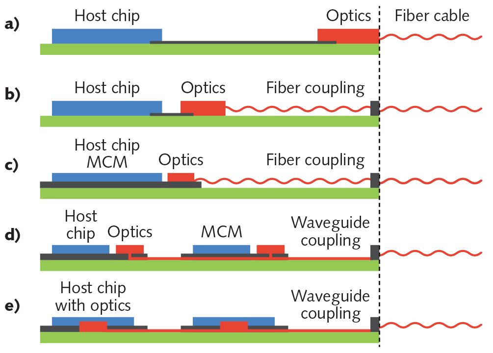
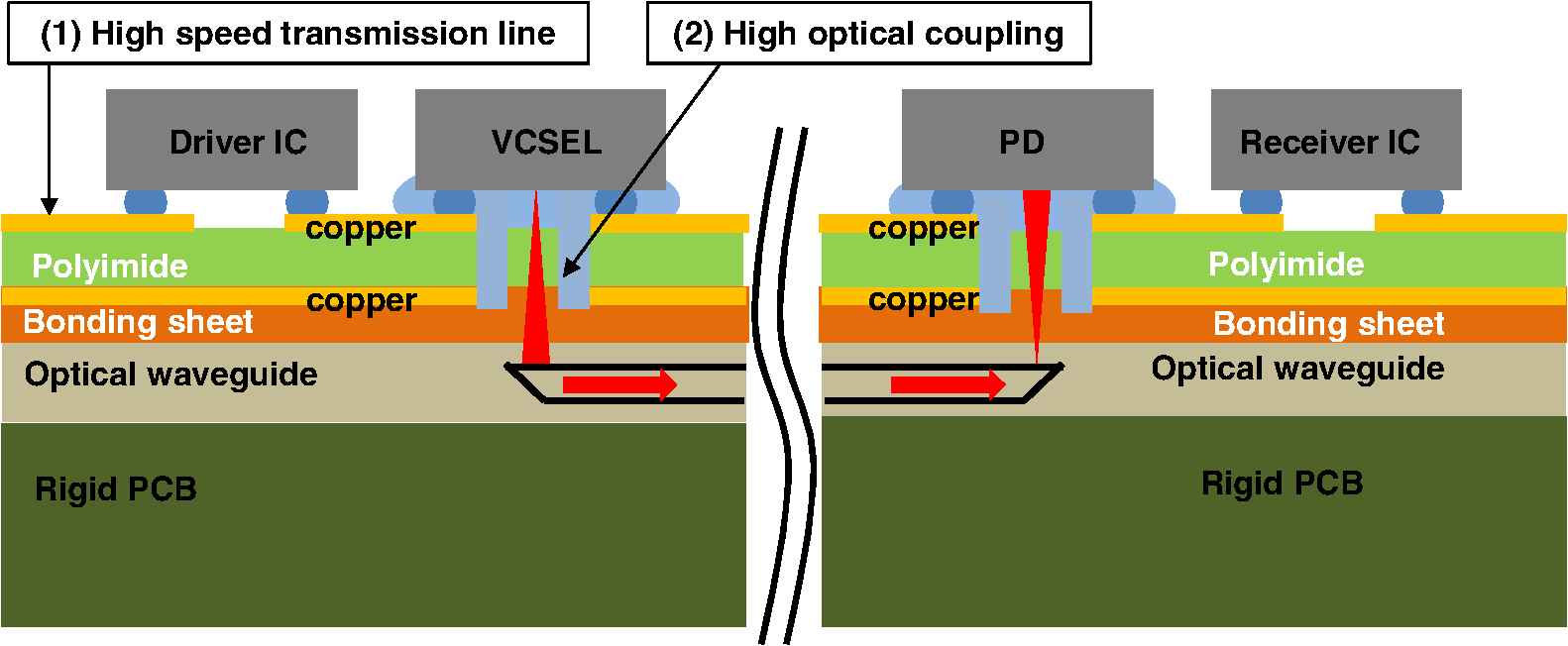
Integrated photonics enables higher bandwidth for data transmission on a PCB. Examples here include data transmission through printed electrical connections (a); short electrical connections between chip and EO transceiver connected with flyover cable (b); multichip-module (MCM) and transceiver on interposer, connected with flyover cable (c); optical signal transmission in the EOCB by optical waveguides (d); and transceiver integrated in the chip sends data into the EOCB-integrated optical waveguides (e).
The goal of the ongoing development is the integration of optical transmission paths into the printed circuit board (PCB), creating a hybrid electrical-optical PCB. Future bandwidth needs forces the development of optical integrated waveguides on board level.
The structure of an EOCB
To build up an EOCB, the glass sheets can be laminated with conventional organic base material such as FR4. Two different structures can be used together: Glass can be a core layer inside the conventional PCB base material (glass core), and glass can be used as the main carrier (a photonic interposer carrying all the PIC and electronic chip components). Copper can be plated on the glass and the organic material. The processing is compatible with regular PCB processing, but needs high-precision assembly.
Figure 2a shows the structure of a typical EOCB. The blue layer in the EOCB denotes a glass layer with integrated single-mode optical waveguides. The electrical processor is located on a glass interposer with a cooling surface on top. A critical point is the connection between the transceiver and the glass layer. Structuring through-glass electrical vias (TGVs) is an established process, but steering the photonic signals is the challenge. Currently, there are at least two techniques under development—either a periscope placed from the top or a small mirror positioned from the bottom of the EOCB. The industry has not yet established standards or multisource agreements for either of these techniques.
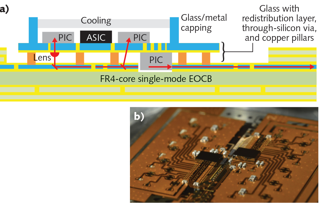
Several different design issues have to be solved for such an EOCB. These include electrical, where RF and electrical signal transmission need path optimization and signal-reflection removal; optical, where signal optimization, free-space collimation, and optomechanical system design must be considered; and thermal, where heat sources have to be regarded and sinks have to be integrated if necessary.
The result of such efforts is shown in Figure 2b. This is a fully operational photonic interposer for an onboard optical transceiver with 25 Gbit/s/ch transmission. A galvanic wafer-level process has been used for making TGVs. On the bottom side of the interposer, polymer lenses have been placed at the ends of the vertical optical pathways in glass—these collimate the light from vertical-cavity surface-emitting lasers (VCSELs) or other light sources on top of the interposer into free space. These signals can be captured by a deflecting mirror element on the underlying structure.
The system shown has very low optical losses of 0.5 dB in the receiver and <2 dB loss measured over a 2 mm distance from the polymer microlens on the transmitter side.
Manufacturing Optical PCBs
The manufacturing process is really many separate processes working together: The glass is first cut into a manageable size and then covered with a metal layer. That metal layer is then coated with a photoresist. After the photoresist has been deposited, a laser direct imaging system writes the required structures into the photoresist, which is then developed and the metal is etched through the resulting openings. Afterwards the photoresist is removed, and the entire glass panel is put into a molten salt, containing silver ions, where an ion-exchange happens between the sodium ions in the glass and the silver ions from the molten salt. Those silver ions create a higher refractive index in the glass. A second reverse ion-exchange follows next to bury the waveguides into the glass. Finally, a CO2 laser is used to cut the glass into the finished boards. The CO2 laser guarantees the optical facet quality we need, so no polishing is required at the end.
Engineers use photolithography and film processing techniques to fabricate the flexible optical waveguides that will be able to move light around components onboard. According to technical information available, waveguides in the build will need walls at least 100 µm thick, and a bend radius less than 5 mm. These dimensions would allow designers to place the waveguide within connectors. This will also let light travel between a line-card and a backplane, without the necessity to convert it to an electrical signal.
PCB Manufacturers usually follow two different techniques when constructing the waveguides—non-contact mask lithography and direct laser writing. In non-contact mask lithography, spin coating applies the material to the substrate. However, as this process is more applicable to semiconductor manufacturing, lithography is better suited for small areas, and cannot be scaled up to handle large areas. Engineers use a process of draw-down coating for large areas, along with a doctor blade.
However, engineers faced two problems with the above process. One, the waveguide material would curl up, requiring 170 g of force to flatten. Second, there was the difficulty of the waveguide adhering to the substrate. Adhesion to the substrate is important so the waveguide would not crack during mechanical process such as cutting the wafer or the substrate board.
It is important to have waveguides that do not attenuate the light too much as it travels through. Optical power measurements made with laser diodes as a source and a photo detector as the receiver indicate onboard waveguides introduce optical losses ranging from 0.046-0.050 dB/cm, even when the waveguides were bent to form two or three loops. Some signal loss is customary from wall roughness within the waveguide as well.
Julian Schwietering explained process followed by Fraunhofer. The manufacturing process is really many separate processes working together: The glass is first cut into a manageable size and then covered with a metal layer. That metal layer is then coated with a photoresist. After the photoresist has been deposited, a laser direct imaging system writes the required structures into the photoresist, which is then developed and the metal is etched through the resulting openings. Afterwards the photoresist is removed, and the entire glass panel is put into a molten salt, containing silver ions, where an ion-exchange happens between the sodium ions in the glass and the silver ions from the molten salt. Those silver ions create a higher refractive index in the glass. A second reverse ion-exchange follows next to bury the waveguides into the glass. Finally, a CO2 laser is used to cut the glass into the finished boards. The CO2 laser guarantees the optical facet quality we need, so no polishing is required at the end.
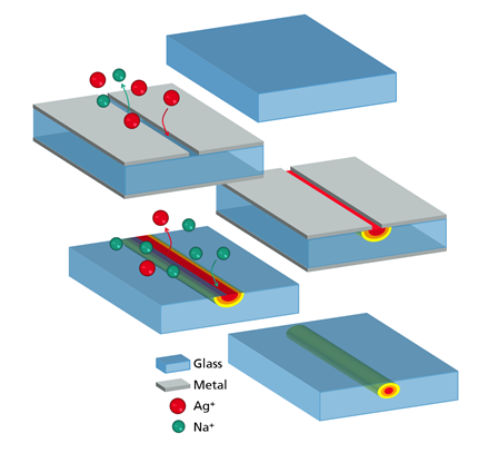
Schematic process of glass-integrated waveguides produced using an ion-exchange technique © Fraunhofer IZM
So far, the biggest challenges were to get the manufacturing process safe and stable, and to minimize attenuation. In the wavelength range of 1550 nanometers, we were able to achieve a minimum propagation loss of 0.06 dB per cm, with high homogeneity across the panel, said Julian Schwietering. One issue we’re pursuing currently is the reduction of propagation losses in the curved sections of the waveguides. Achieving smaller bend radii allows higher integration density of the optical circuits. Future challenges will include the development of connector concepts. Circuit boards should be connectable both at the edges and on the surface of the glass. We have different approaches under evaluation that could achieve the coupling for a wide range of wavelengths with low coupling losses.
Making waveguides in display glass
An essential technology for EOCB is the fabrication of waveguides in the glass layer, which can be seen as the optical analog to printing circuits on a PCB. Waveguides can be tailored for single-mode (SM) or multimode (MM) transmission. While many datacom structures are working with multimode signals, silicon photonics is mostly based on the use of single-mode signals, which will be the focus of the following.
Waveguides in glass can be produced by lasers or by other technologies such as ion-exchange processes that originate from semiconductor processing. The latter have the advantage of parallel processing, while laser processes are inherently sequential because the laser has to follow the path of the waveguide.
Glass-integrated optical waveguides fabricated by ion-exchange in large-sized thin glass © Fraunhofer IZM
The thermal (silver) ion-exchange process is well established for the creation of waveguides at a wafer level. At Fraunhofer IZM (Berlin, Germany), this procedure for integrated optics has been transferred to full panel level at sizes up to 610 mm × 440 mm. It has also been modified from a reliance on special glasses towards the use of cost-effective display glass. The whole process has been configured for large-scale manufacturing.
References and Resources also include:
https://www.rushpcb.co.uk/2018/01/optical-printed-circuit-boards/
https://blog.izm.fraunhofer.de/the-glassy-future-of-circuit-boards/