 International Defense Security & Technology Your trusted Source for News, Research and Analysis
Related Articles

“We’re not just discovering materials—we’re inventing them atom by atom. Metamaterials represent the ultimate triumph of structure over substance.”
— Dr. David Smith, Duke University, Pioneer of the First Invisibility Cloak
Beyond Nature’s Limits: Redefining Material Possibilities
In the world of materials science, a groundbreaking revolution is underway, driven by the emergence of metamaterials. Metamaterials—artificially structured materials with properties not found in nature—are unlocking new dimensions of control over electromagnetic waves, sound, heat, and even seismic vibrations. Engineered at the nanoscale, they challenge conventional boundaries in physics by altering how waves interact with matter. Metamaterials hold immense promise in a range of applications, from superlenses and superfast optical networks to EMI suppression and wireless charging.
As of 2025, the global metamaterials market is valued at $2.08 billion, with forecasts estimating it will reach $15.36 billion by 2034. This exponential growth is fueled by applications across 6G telecommunications, aerospace defense systems, quantum computing, and beyond.
In this article, we will explore the incredible potential of metamaterials and how they are reshaping various industries.
What are Metamaterials
Core Innovations: From Theory to Industrial Reality
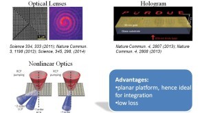
Light and Electromagnetic Mastery
Acoustic and Seismic Control
Sound and vibration metamaterials are enabling architectural silence and seismic protection. Acoustic metamaterials are engineered structures designed to manipulate, direct, and control sound waves in ways that natural materials cannot. By leveraging unique properties such as negative mass density or negative bulk modulus, these materials enable advanced applications including acoustic cloaking, super-resolution imaging (acoustic super-lensing), noise cancellation, and sound wave confinement. Recent developments have extended their utility across industries—from architectural acoustics and noise reduction systems to medical imaging and non-destructive testing—where precise sound control is essential.
Energy and Thermal Engineering
In energy applications, metamaterials are enabling passive cooling and wireless power transmission. Researchers at the University of Colorado have developed radiative cooling films using glass-polymer-silver structures that lower temperatures below ambient levels without electricity. Composed of a polymer matrix embedded with glass microspheres and coated with a thin layer of silver, the film achieves high solar reflectivity and strong infrared emissivity. This combination allows it to cool objects beneath ambient air temperature even under direct sunlight. The breakthrough addresses the long-standing challenge of balancing solar reflection with thermal emission and holds significant promise for energy-efficient cooling in buildings, power plants, vehicles, and electronic devices, potentially reducing reliance on conventional air conditioning systems. These have shown HVAC energy savings of 30% in Arizona pilot trials.
Additionally, resonant metamaterial couplers now allow efficient mid-range wireless power transfer, overcoming alignment issues faced by traditional coil-based systems, and powering remote sensors and wearable devices.
Sector Transformations: 2025’s Frontier Applications
Defense and Aerospace
Defense systems are among the earliest adopters of metamaterial innovation. Technologies such as electromagnetic cloaking and signature deflection are redefining stealth capabilities for aircraft, ships, and drones. India’s Analakshya MSCS exemplifies radar wave redirection, while Echodyne’s ultra-compact metamaterial radar units reduce payload by 40% without sacrificing resolution—ideal for drones and autonomous platforms.
Healthcare
In the medical field, metamaterials are enhancing diagnostics and imaging. Metasurface coils used in MRI machines have demonstrated a 30% improvement in signal-to-noise ratio, allowing for more precise detection of tumors and other anomalies. Meanwhile, terahertz biosensors built on metamaterial substrates are enabling detection of diseases at the molecular level, making real-time, non-invasive diagnostics a clinical reality.
Telecommunications
Telecom giants are rapidly investing in metamaterial-enabled infrastructure to realize terabit-speed 6G networks. Researchers at Caltech have demonstrated terahertz modulators that can operate at unprecedented bandwidths, while companies like Kymeta are revolutionizing satellite internet with their low-profile, flat-panel antennas integrated into vehicles and aircraft.
Manufacturing Breakthroughs: Scaling the Impossible
Researchers at the Hasso Plattner Institute in Germany have pushed the boundaries of metamaterials by designing them as fully functional mechanical machines rather than static materials. Through advanced 3D printing techniques, they have created metamaterial mechanisms capable of performing complex mechanical tasks—such as a door latch that converts rotary motion into linear movement and a walking mechanism built from a single block of interconnected metamaterial cells. Central to these innovations is the use of specialized shear cells, which enable precise mechanical behavior within the material’s structure.
To streamline the design process, the team developed a dedicated 3D editor that allows users to integrate various types of functional cells, including shear cells, directly into their metamaterial designs. This editor features simulation tools that apply forces and visualize deformations, empowering designers to optimize mechanical performance before fabrication. With metamaterial-enabled devices spanning applications across radio frequency (RF), terahertz (THz), infrared (IR), and visible light spectra, this approach heralds a new era of engineering where materials themselves act as sophisticated machines, unlocking transformative possibilities in robotics, adaptive structures, and beyond.
Recent advances in nanomanufacturing have significantly reduced the cost and increased the scalability of metamaterials. Nanoimprint lithography (NIL) is enabling the production of 300mm wafers with metasurface patterns at <$0.50 per lens at scale. Equipment from EV Group now achieves production yields exceeding 95% for consumer electronics. Meanwhile, AI-driven design platforms like PlanOpSim accelerate the discovery of new metamaterials by simulating millions of structures per day, bypassing traditional trial-and-error. Hybrid fabrication techniques, which blend atomic layer deposition with roll-to-roll printing, are unlocking mass production of large-area and flexible metasurfaces for smart clothing, packaging, and solar panels.
Quantum Horizons: The Next Leap
At the intersection of quantum science and metamaterials, 2025 is poised to be a defining year. At META 2025 in Malaga, researchers will present advancements in topological photonics, where silicon-boron nitride waveguides offer defect-tolerant light propagation essential for quantum computing. DARPA-backed entanglement metasurfaces are also entering early trials, capable of focusing photon pairs into structured quantum states for secure communication networks and photonic quantum processors.
“Meta-optics are the integrated circuits of photonics. Just as transistors miniaturized electronics, metalenses will collapse all optical systems onto chips.”
— Federico Capasso, Harvard University
Global Leaders and Market Dynamics
Chinese Advancements
Sustainability Frontiers
Metamaterials also play a pivotal role in sustainability. Passive cooling films, inspired by Saharan silver ants, reflect infrared radiation to reduce refrigeration energy needs. In solar energy, Phomera’s photonic crystals, backed by BASF, increase light trapping in solar panels, boosting efficiency by 15%. Additionally, MIT’s 3D-printed architected materials, developed by Carlos Portela’s lab, deliver strength-to-weight ratios 200% higher than steel, enabling lighter, more sustainable structural components in buildings and vehicles.
Challenges and Future Outlook
Conclusion: The Engineered Future
Metamaterials have evolved from academic curiosities into strategic technologies shaping our engineered future. They now power polarization-sensing smartphone cameras, reinforce earthquake-resilient buildings, enhance MRI performance, and enable ubiquitous satellite internet. With the convergence of AI design tools, scalable nanofabrication, and growing industry demand, metamaterials are redefining what’s possible in optics, acoustics, defense, and sustainability.
The metamaterials revolution is no longer on the horizon—it’s embedded in your devices, shielding your infrastructure, and illuminating the quantum future.
Stay informed and engage with the forefront of innovation at Metamaterials’2025 (Sept 1–4, Amsterdam) and META 2025 (July 22–25, Malaga).
References and Resources also include:
- http://www.latimes.com/science/sciencenow/la-sci-sn-tiny-invisibility-cloak-gold-metamaterial-20150917-story.html
- https://www.eda.europa.eu/info-hub/press-centre/latest-news/2015/11/26/seminar-on-metamaterials-for-defence-applications
- http://eda.europa.eu/what-we-do/activities/activities-search/metamaterials-for-active-electronically-scanned-arrays-(metalesa)
- http://phys.org/news/2016-11-semiconductor-free-microelectronics-metamaterials.html?utm_source=nwletter&utm_medium=email&utm_campaign=weekly-nwletter
- https://www.parc.com/services/focus-area/metamaterials/
- https://www.emergenresearch.com/industry-report/metamaterials-market
- https://www.precedenceresearch.com/metamaterials-market