 International Defense Security & Technology Your trusted Source for News, Research and Analysis
Related Articles

Introduction:
The aerospace and defense industries are at the cutting edge of innovation, constantly striving to push the boundaries of technology to enhance safety, security, and performance. These sectors require sophisticated systems that meet the highest standards of reliability and precision. Electronic Design Automation (EDA) is a critical enabler of this progress, providing the tools and methodologies that allow engineers to design, simulate, and verify the complex electronic systems at the heart of modern aerospace and defense technologies. This article explores how EDA is empowering these industries, enabling faster, more efficient, and reliable design processes.
EDA: The Backbone of Modern Electronic Design
Electronic Design Automation (EDA) is the backbone of modern electronic design. EDA tools, also known as Electronic Computer-Aided Design (ECAD), offer a more efficient and streamlined approach to designing electronic systems, including integrated circuits and printed circuit boards. Historically, manual techniques such as photoplotters were used to create circuit board drawings. However, as designs became more complex, automation became necessary. EDA tools emerged to assist with drafting, place and route, and functional verification.
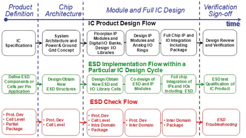
Electronic products must meet strict guidelines for their intended operating environments as well as for manufacturability, and in a number of industries products have to meet a set of complicated regulatory standards. To overcome these complexities, a next-generation design platform must support integration, shared data and improved intelligence. Integration across design processes and disciplines optimizes resources to reduce development time and cost.
One of the key benefits of EDA tools is their ability to enhance the construction of electronic components by identifying and eliminating bugs and defects. Through universal design techniques, these tools help ensure that chips and circuit boards are error-free and meet the required specifications. This is crucial, as errors in manufactured chips can be catastrophic, often necessitating a complete redesign and re-manufacturing, resulting in significant time and cost implications.
As the electronics industry enters a new era of digital transformation, these technologies are fundamentally changing the way businesses operate. This digital shift is particularly impactful in aerospace and defense, where the integration of mechanical and electrical design processes is essential. EDA tools streamline this entire process, from product inception to manufacturing, ensuring that electronic products meet stringent guidelines for their operating environments and adhere to complicated regulatory standards.
The Complexity of Modern Semiconductor Chips
State-of-the-art semiconductor devices are incredibly intricate, often containing over a billion circuit elements. The interactions between these elements can be subtle and complex, with variations in the manufacturing process introducing additional layers of complexity. Managing this level of detail is impossible without sophisticated automation, which is where EDA tools come into play. These tools provide the critical technology needed to design and manufacture today’s semiconductor devices, ensuring that they meet the necessary specifications and performance criteria. The increasing demand for advanced electronic devices with complex designs, coupled with the need to reduce the size while enhancing the performance of integrated circuits (ICs), is compelling manufacturers to ramp up their research and development (R&D) investments in EDA tools.
Meeting the Challenges of Modern Aerospace and Defense
Modern aerospace and defense systems are highly complex, integrating a wide range of components and technologies. EDA tools excel in managing this complexity, allowing designers to seamlessly integrate analog, digital, RF, and mixed-signal components. They provide methodologies for designing multi-domain systems and tools for efficient collaboration among various engineering disciplines.
Electronic Design Automation encompasses a suite of software tools used to design, verify, and simulate electronic systems, including integrated circuits (ICs), printed circuit boards (PCBs), and embedded systems. In the aerospace and defense industry, where reliability, precision, and performance are paramount, EDA tools provide the essential backbone for creating systems that meet these stringent requirements.
The development of avionics systems, radar and communication systems, navigation, and control systems all rely heavily on EDA. These tools enable engineers to design and simulate complex electronic architectures before physical prototypes are built, significantly reducing time-to-market and development costs. Moreover, EDA helps ensure that these systems can operate in the harsh environments often encountered in aerospace and defense applications, such as extreme temperatures, high levels of radiation, and electromagnetic interference.
The aerospace and defense industry faces unique challenges that require specialized solutions. One of these challenges is the need for systems that can operate reliably over extended periods without maintenance. EDA tools provide the means to design systems with built-in redundancy and fault tolerance, ensuring that they can continue to function even in the event of component failures.
Another challenge is the increasing complexity of electronic systems in modern aircraft and defense platforms. As systems become more interconnected and data-intensive, EDA tools offer the capability to manage this complexity through advanced simulation and verification techniques. These tools allow engineers to model the interactions between different subsystems, ensuring that they work together seamlessly and that potential issues are identified and addressed early in the design process.
Enhancing Design Efficiency and Innovation
EDA tools revolutionize the design process by providing advanced features for modeling, simulation, and optimization. These tools enable designers to create complex electronic systems, such as avionics and defense systems, with greater efficiency and accuracy. EDA tools facilitate system-level design exploration, architectural analysis, and optimization, leading to designs that meet stringent requirements while reducing development time and cost.
One of the key advantages of EDA in the aerospace and defense sector is its ability to streamline the design process. Traditional design methods are often time-consuming and prone to errors, but EDA tools automate many of these processes, allowing engineers to focus on innovation rather than repetitive tasks.
EDA tools also significantly reduce development time and cost by allowing designs to be simulated and analyzed before hardware is purchased and manufactured. This helps identify and rectify any issues or inefficiencies early in the design process. Additionally, computer-aided manufacturing (CAM) tools are used in the manufacturing stage to control automated machinery based on the design data generated by the EDA tools, thus transforming the design concept into a physical product.
Computer-aided engineering and Computer-Aided Design
Within the realm of electronic design, there are two main categories of tools: computer-aided engineering (CAE) and computer-aided design (CAD). CAE tools focus on the design and analysis of electronic elements, enabling simulations, analysis, and verification of design decisions. On the other hand, CAD tools aid in producing the physical layout of the circuit board, facilitating the placement of components, clearance verification, thermal analysis, and supporting manufacturing processes.
ECAD systems, which fall under CAD, play a crucial role in the design and analysis of electronic elements in a product. These systems leverage the availability of online libraries containing vast component data and integrate circuit simulation functionality, enabling designers to quickly and accurately verify their design decisions. By simulating the behavior of electronic circuits, designers can ensure that their designs meet performance and reliability requirements.
Once the design has been verified, ECAD systems assist in generating a printed circuit board (PCB) layout. This process is significantly faster and more efficient compared to traditional manual techniques. The system optimizes the placement of components, taking into account factors such as signal integrity, power distribution, and thermal management. Visual representations of the completed layout provide crucial information for tasks like enclosure clearance verification, thermal analysis, and support for electronics manufacturing processes.
The feedback loop between these supporting engineering activities and the circuit design process is a vital aspect of ECAD systems. Any conflicts or issues identified during enclosure clearance verification, thermal analysis, or manufacturing considerations can be integrated back into the circuit design process. This allows designers to make necessary adjustments, refinements, or even complete redesigns to ensure optimal performance, reliability, and manufacturability of the electronic system.
Overall, EDA tools play a vital role in the electronic design process, offering improved efficiency, accuracy, and cost-effectiveness. They have revolutionized the way electronic systems are designed, verified, and manufactured, enabling the realization of innovative and reliable products in industries such as aerospace and defense.
EDA also facilitates the integration of emerging technologies, such as artificial intelligence (AI) and machine learning (ML), into aerospace and defense systems. By leveraging AI-driven design automation, engineers can optimize system performance, reduce power consumption, and enhance overall efficiency. This capability is particularly important in the development of autonomous systems, where AI and ML play a crucial role in enabling real-time decision-making and adaptive behavior.
Overall, the integration of CAE and CAD tools within the EDA framework empowers designers in the electronic design process. It enables faster and more accurate verification of design decisions, efficient PCB layout generation, and seamless collaboration between design and supporting engineering activities. ECAD systems are indispensable in optimizing the electronic design process, leading to improved product quality and reduced time to market.
For in-depth understanding on EDA technology and applications please visit: Comprehensive Guide to Electronic Design Automation (EDA): Tools, Techniques, and Applications
Verification, Validation, and Power Optimization
For instance, EDA tools can automatically generate and verify the layout of PCBs, ensuring that components are correctly placed and that signal integrity is maintained. This automation reduces the likelihood of human error, which is critical in the development of systems where even a minor mistake can lead to catastrophic failures.
Reliability and safety are paramount in aerospace and defense applications. EDA tools offer advanced verification and validation techniques, ensuring that designs adhere to specifications and standards. Techniques such as formal verification, assertion-based verification, and coverage analysis help identify potential design flaws, reducing the risk of errors or failures during operation.
Power optimization is another critical concern in aerospace and defense, where strict power constraints and the need for energy efficiency are constant challenges. EDA tools provide capabilities for power optimization, including dynamic power management, voltage scaling, and leakage power reduction. By accurately analyzing and optimizing power consumption, these tools help extend battery life, reduce heat dissipation, and enhance overall system performance.
Manufacturing and Testing in Aerospace and Defense
EDA tools also address challenges related to manufacturing and testing in aerospace and defense systems. Design for Manufacturability (DFM) features ensure that designs are robust against process variations, lithography challenges, and manufacturing constraints. Additionally, EDA tools support testability features, such as automated test pattern generation and built-in self-test (BIST), making it easier to test complex systems efficiently.
Ensuring Security and Compliance
In the aerospace and defense sector, security is of paramount importance. EDA tools play a critical role in ensuring that electronic systems are secure and compliant with industry standards and regulations.
Security is a top concern in aerospace and defense applications. EDA tools are evolving to incorporate features for hardware security, secure communication, and encryption, enabling designers to implement robust security measures and perform vulnerability analysis to mitigate potential risks. These tools enable the design of secure architectures, the implementation of encryption and authentication mechanisms, and the verification of compliance with standards such as DO-254 for airborne electronic hardware.
Moreover, as cyber threats continue to evolve, EDA tools are essential for designing systems that are resilient to attacks. By incorporating security features at the design stage, engineers can protect critical systems from potential vulnerabilities that could be exploited by adversaries.
Collaboration, and Standardization
Collaboration and standardization are essential in the aerospace and defense industries, where diverse teams work together to create cutting-edge technologies. EDA tools facilitate seamless collaboration by enabling efficient sharing of design data and fostering innovation. Standardization efforts, such as interoperability standards and open-source initiatives, promote tool compatibility and facilitate the exchange of design information.
ECAD Tools
Comparing the features, advantages, and applications of various ECAD (Electronic Computer-Aided Design) tools helps in understanding their specific roles in electronic design and their unique benefits. Here’s a detailed comparison of some prominent ECAD tools:
1. Altium Designer
Features:
- Unified Design Environment: Integrates schematic capture, PCB layout, and component management in a single platform.
- Advanced Routing: Offers advanced routing features such as interactive and auto-router tools.
- 3D Visualization: Provides real-time 3D visualization of PCB designs.
Advantages:
- Seamless Workflow: The unified environment reduces the need for data conversion between different tools, improving efficiency.
- Enhanced Design Accuracy: Advanced routing and design rule checks help prevent errors and improve design accuracy.
- User-Friendly Interface: Intuitive interface and powerful design tools streamline the design process.
Applications:
- Consumer Electronics: Widely used in designing complex consumer electronic devices such as smartphones and tablets.
- Medical Devices: Suitable for creating precise and reliable designs for medical electronics.
- Automotive: Helps in designing automotive electronics with complex requirements.
2. Cadence Allegro
Features:
- High-Performance Layout: Provides tools for high-speed PCB and IC package design.
- Advanced Simulation: Includes tools for signal integrity, power integrity, and thermal analysis.
- Integrated Design: Supports a complete design flow from schematic entry to PCB layout and verification.
Advantages:
- Robust Analysis: Advanced simulation tools ensure the design meets performance and reliability standards.
- Scalability: Suitable for both small-scale designs and large, complex systems.
- Collaborative Features: Enhanced support for team collaboration and design data management.
Applications:
- Aerospace & Defense: Used for high-reliability designs in aerospace and defense applications.
- High-Speed Digital Designs: Ideal for designing high-speed digital and RF circuits.
- Industrial Automation: Supports the design of control systems and other industrial electronic systems.
3. Mentor Graphics PADS
Features:
- Scalable Solutions: Offers scalable solutions from basic PCB design to advanced design capabilities.
- Design Rule Checking: Includes comprehensive design rule checking and error detection.
- Library Management: Advanced library management and component creation tools.
Advantages:
- Flexible Licensing: Provides flexible licensing options for different scales of operations.
- Ease of Use: User-friendly interface with a range of features suited for various design needs.
- Integrated Tools: Seamless integration with simulation and analysis tools.
Applications:
- Consumer Electronics: Popular for designing a wide range of consumer electronic products.
- IoT Devices: Suitable for designing Internet of Things (IoT) devices with varied requirements.
- Telecommunications: Used in designing telecom equipment and systems.
4. KiCad
Features:
- Open Source: Free and open-source tool with no licensing costs.
- Cross-Platform: Available on multiple operating systems including Windows, Linux, and macOS.
- Extensive Libraries: Provides a wide range of libraries and footprints for different components.
Advantages:
- Cost-Effective: No licensing fees make it an attractive option for small businesses and hobbyists.
- Community Support: Strong community support and frequent updates from contributors.
- Customizability: Allows users to customize and extend the tool as needed.
Applications:
- Hobbyist Projects: Ideal for individual designers and hobbyists working on personal projects.
- Educational Use: Widely used in educational settings for teaching PCB design principles.
- Prototyping: Suitable for small-scale prototypes and early-stage product development.
5. Autodesk Eagle
Features:
- User-Friendly: Intuitive interface with easy-to-learn tools for schematic capture and PCB layout.
- Cloud Integration: Offers cloud storage and collaboration features.
- Component Libraries: Includes a large library of components and symbols.
Advantages:
- Ease of Use: Designed for ease of use with a low learning curve, making it accessible to beginners.
- Collaboration: Cloud-based features facilitate team collaboration and version control.
- Affordability: Cost-effective pricing for professional and educational use.
Applications:
- Startup Projects: Popular among startups and small businesses for rapid prototyping.
- Educational Institutions: Used in educational institutions for teaching PCB design.
- DIY Electronics: Ideal for DIY enthusiasts and hobbyists working on electronic projects.
Summary
- Altium Designer is known for its integrated design environment and advanced routing capabilities, making it suitable for complex and high-performance designs.
- Cadence Allegro excels in high-speed and high-reliability designs with robust simulation tools, making it ideal for aerospace, defense, and industrial applications.
- Mentor Graphics PADS offers scalable solutions with strong design rule checking and library management, suitable for various industrial and consumer applications.
- KiCad provides a cost-effective, open-source solution with strong community support, ideal for hobbyists and educational use.
- Autodesk Eagle is user-friendly and cloud-integrated, making it a popular choice for startups, educational institutions, and DIY enthusiasts.
Each ECAD tool has its strengths and is suited to different types of design projects and user needs, ranging from high-performance industrial applications to educational and hobbyist use.
The Future of EDA in Aerospace and Defense
As the aerospace and defense industry continues to evolve, the role of EDA will become even more significant. The rise of next-generation technologies, such as quantum computing, hypersonic systems, and space exploration, will present new challenges and opportunities for EDA. These tools will be instrumental in enabling the design of systems that can operate in extreme environments, handle unprecedented levels of data, and meet the rigorous demands of future defense applications.
Conclusion
Electronic Design Automation (EDA) is at the heart of the future of aerospace and defense. By providing advanced tools for design, verification, validation, and optimization, EDA empowers engineers to create the sophisticated electronic systems that are critical to the safety, security, and performance of modern aerospace and defense technologies.
As technology continues to advance, the partnership between EDA and the aerospace and defense sector will remain a driving force behind some of the most significant innovations of our time. As the industry continues to evolve, EDA will remain a crucial enabler of innovation, helping to push the boundaries of what is possible in these vital fields.
References and Resources also include:
https://www.lifecycleinsights.com/tech-guide/ecad/