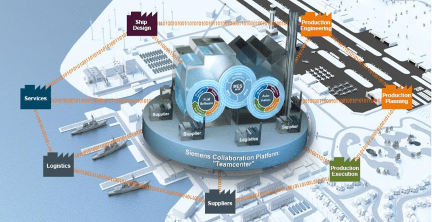
Home / Industry / Pioneering the Future: Harnessing the Power of 2D Nanomaterials for Revolutionary Technologies

Pioneering the Future: Harnessing the Power of 2D Nanomaterials for Revolutionary Technologies

Introduction:

In the ever-evolving landscape of technological innovation, 2D nanomaterials have emerged as a game-changing class of materials with extraordinary properties, paving the way for advancements across diverse fields. From revolutionizing high-speed electronics to enhancing military surveillance, energy storage devices, and even armors and weapon systems, these ultrathin wonders are at the forefront of cutting-edge research and development. In this article, we delve into the immense potential of 2D nanomaterials and their transformative impact on various fields, from electronics to military applications and beyond.

The Rise of 2D Nanomaterials

Silicon, the cornerstone of modern electronics, is nearing its technological limits, prompting researchers to explore alternative materials. One such groundbreaking class is 2D nanomaterials, defined by their astonishingly thin structure, with a mere one or two atoms thickness.

What are 2D Nanomaterials?

2D nanomaterials refer to materials that are only a few atoms thick, with graphene being the most well-known example. These materials exhibit exceptional mechanical, thermal, and electrical properties owing to their unique atomic structure.

2D nanomaterials, with their unique atomic structure, allow electrons to move freely within a two-dimensional plane, governed by quantum mechanics. Notable examples include graphene, a single layer of carbon atoms arranged in a hexagonal lattice, and other emerging materials like MoS2, hBN, WS2, and WSe2.

Graphene – The Pioneer:

Graphene, a single layer of carbon atoms arranged in a hexagonal lattice, has set the stage for the exploration of 2D nanomaterials. Its exceptional conductivity, mechanical strength, and flexibility have sparked a revolution in material science and various industries. We now find it in composites with enhanced mechanical or thermal properties, batteries, inks for printable electronics, photodetectors and some chemical and biological sensors. Other products inlude, such as solar cells, flexible devices, supercapacitors, water filters/desalinators and neural interfaces.

New Enrants

However Graphene lacks a bandgap, the key property required to create transistors, logic and memory circuits. In recent years, new materials such as molybdenum disulfide, has been researched as a substitute for graphene and silicon. The monolayer molybdenum disulfide (MoS2), one of the promising 2D materials with a direct bandgap has high potential for applications in nano electronic devices, energy storage, photocatalysts, and chemical sensors. Molybdenum disulfide  is a  new 2-D material , consisting of a single-atomic layer of molybdenum sandwiched between two adjacent atomic layers of sulfide. This compound exists abundantly in nature as the mineral molybdenite, a crystal material found in rocks around the world, frequently taking the characteristic form of silver-colored hexagonal plates. The material has been used for many years as an industrial lubricant for aircraft and motorcycle engines.

MXenes are other kinds of 2D materials with higher saturable absorption (SA) than the other 2D materials. Having higher SA (up to 50%) provides increased modulation depth for optical isolator applications. 2D transition metal carbides, nitrides or carbonitrides have been introduced as MXene with a chemical formula of 1 M YnTx n + , where M is the transition metal (such as Sc, Ti, Zr, Hf, V, Nb, Ta, Cr, Mo, Mn ), Y is the carbon or nitrogen, T is the functional groups such as =O or -OH (n=1-3). They are produced by extracting the Y element from three-dimensional (3D) MYT phases with acidic chemical reactions.

Each of them has different properties that can be used in the different application fields; for example, graphene is found to be an excellent electrical conductor whereas hBN is an insulator with a large bandgap. However, contrary to electric conduction, hBN has better tribological properties than graphene, especially in high temperatures. MoS2 with different electrical, chemical, biological, and mechanical properties than other 2D materials are used in electronics, catalysis, biomedical, and energyrelated fields as nanosheets. Semiconductor MoS2 can retrieve the weakness of the graphene band gap and is used in optoelectronic applications.

Purdue University researchers have unveiled a groundbreaking two-dimensional nanomaterial, named tellurene, derived from tellurium. This nanomaterial exhibits unique properties and holds promise for applications in high-speed electronics, military surveillance tools, and biochemical detection devices. The researchers overcame challenges associated with the reliable production of two-dimensional crystals, creating tellurene in a solution with a thin and durable structure. Wenzhuo Wu, an assistant professor at Purdue’s School of Industrial Engineering, emphasized the material’s superiority over other two-dimensional materials due to its high production yield and air stability.

Tellurene’s potential applications include incorporation into surveillance equipment, airport scanners, night-vision devices, and high-speed transistors for national defense tools. Wu’s team has demonstrated high-performance transistors and is actively developing tellurene-based infrared technologies, emphasizing its affordability and flexibility compared to current electronic devices. The material’s sensitivity to temperature variations positions it as a key component for biosensors in airports, offering potential applications in detecting communicable diseases based on body temperature differences. This breakthrough was recently published in Nature Electronics, marking a significant stride in the development of versatile and impactful nanomaterials.

Applications Across Industries

Such attributes position 2D nanomaterials as frontrunners in revolutionizing electronics, energy storage, military surveillance, and defense systems.

Two-dimensional materials have extraordinary properties such as extremely low resistance or highly efficient interactions with light. Because of these properties they could have big role in the fight against climate change. Eight percent of global electricity consumption in 2020, was due to information technologies, including computers, smartphones and large data centres of tech giants such as Google and Amazon. That figure is projected to double every decade as demand for AI services and smart devices skyrockets. Using 2D materials to make more efficient devices will have advantages of reduced carbon emissions, says Mr Wurdack a PhD student in the Nonlinear Physics Centre (NLPC) of the Research School of Physics .

1. High-Speed Electronics

The ultra-high electron mobility of 2D materials, such as graphene and transition metal dichalcogenides (TMDs), has opened up new frontiers in electronics. These materials promise faster and more energy-efficient electronic devices, challenging the limits of conventional silicon-based technology.

2D nanomaterials are at the forefront of the next wave of electronics. Their potential applications include solar cells, transistors, camera sensors, digital screens, and semiconductors. Advancements in nanoelectronic devices hold the promise of reducing carbon emissions associated with information technologies.

2. Energy Storage Devices

In the realm of energy storage, 2D nanomaterials have demonstrated unparalleled potential. From supercapacitors to batteries, these materials show enhanced performance, addressing the increasing demand for energy storage in devices such as smartphones, electric vehicles, and more.

Graphene-based supercapacitors and batteries show enhanced energy storage capacities, faster charging times, and longer cycle life, addressing critical challenges in portable electronics and electric vehicles.

  • Batteries on Steroids: The high surface area and tunable properties of 2D materials hold immense potential for next-generation batteries. Imagine phones charged in seconds, electric vehicles with extended range, and even grid-scale energy storage solutions.
  • Solar Cells 2.0: 2D materials can harvest sunlight across a wider spectrum than traditional silicon, paving the way for more efficient and flexible solar cells.

Military Applications

Two-dimensional (2D) materials and heterostructured 2D materials have emerged as pivotal elements for diverse military applications, spanning energy storage, sensors, electronic devices, armors, and weapon systems. Advanced 2D material-based sensors and detectors offer heightened awareness, providing crucial data for military planning and decision-making in command and control operations. These materials, known for their crystalline structure consisting of single or few layers of atoms, exhibit superconductivity and are employed in various applications, such as processors, nano/microchips, and cathodes for thermal batteries in missiles and rockets. Research in material science delves into understanding these materials not only at the nanoscale but also under extreme macro-scale conditions.

Graphene, a leading 2D material, possesses unparalleled properties like chemical inertness, high thermal stability, electrical conductivity, and mechanical strength. Its potential applications in military settings include serving as light ballistic armor due to its superior mechanical strength, corrosion resistance for protecting critical components in naval operations, and use in screens and touch panels for harsh operating conditions. The material’s superconductivity allows its utilization in electric/electronic applications like computer processors, antennas, and solar cells. Graphene’s high electrical conductivity and optical transmittance make it suitable for screens, liquid crystal displays, photovoltaic cells, and organic light-emitting diodes, especially in military contexts with demanding conditions.

Moreover, graphene’s application extends to energy storage, as it serves as an electrode material for lithium-ion batteries, enhancing their conductivity and overall capacity. Its use in producing infrared transparent windows for guided missiles and its role as an infrared sensor/detector further highlight its multifaceted utility in military technologies.

Beyond graphene, other 2D materials like hBN and MoS2 exhibit specific strengths. For instance, hBN, despite being an insulator, can enhance fuel cell performance when activated by graphene and serve as a solid lubricant in tribological systems. MoS2 finds application in ultra-fast field-effect transistors, optical devices, and gas sensors, contributing to the development of high-performance military technologies.

The class of MXene 2D materials presents promising avenues for military applications, including photothermal conversion, field-effect transistors, topological insulators, optoelectronic properties, sensors, and hydrogen evolution reactions. Notably, MXene materials offer improved saturable absorption, making them valuable for optical isolator applications in fiber-based femtosecond lasers, relevant to military systems like FLIR cameras and targeting pods. Additionally, their high effective Young’s modulus suggests applications in protective coatings, membranes, and nanoresonators for military purposes. These advancements in 2D materials underscore their transformative potential across a spectrum of military technologies, contributing to enhanced performance, durability, and functionality.


Heterostructured 2D materials, spurred by the pioneering research on graphene derived from graphite exfoliation, have become a focal point in materials research.

These heterostructures involve stacking individual monolayers of diverse 2D materials, such as WSe2, MoTe2, WS2-MoS2, WSe2-SnS2, hBN-graphene, and MoS2-graphene, facilitating excellent electron transfer. This innovation has led to novel avenues in military applications, including transistors, photodetectors, chemical and biological sensors, and nanoelectromechanical systems. Combinations like graphene and black phosphorus exhibit unique light-substance interaction phenomena, promising advancements in infrared detectors for military use. Heterostructured 2D materials also play a crucial role in developing energy storage systems to replace conventional lithium-ion batteries, with graphene-based electrodes like Na+, K+, Mg2+, and Al3+ showing promise. Moreover, the application of these materials in wearable sensing systems and flexible/stretchable electronics holds potential for military applications, providing infantry units with novel sensors and devices. The formation of Moire patterns through the stacking of similarly structured monolayer materials, such as MoS2/MoSe2, offers high electron mobility and great potential for nanodevice development. The exploration of MXenes/graphene heterostructures for battery cathodes further contributes to advancements in energy storage technology. Overall, heterostructured 2D materials present a gateway to quantum-engineered transistors, offering alternatives to traditional silicon technology in sensors, electronic devices, and computers.

Military Surveillance

The unique properties of 2D nanomaterials are particularly advantageous in the development of advanced military surveillance systems. Their lightweight nature, coupled with excellent electrical conductivity, makes them ideal candidates for creating highly sensitive sensors and imaging devices.

Graphene, for instance, is a million times thinner than paper, transparent, and incredibly strong. Researchers at Purdue University have recently discovered tellurene, a 2D nanomaterial with applications in high-speed electronics, defense tools, and biochemical detection, potentially revolutionizing infrared technology.

  • Cloaking, Not Magic: Graphene’s unique ability to manipulate light makes it a potential candidate for camouflage technology, rendering equipment and personnel invisible to specific wavelengths.
  • Seeing Through Walls: 2D materials can be engineered to emit specific frequencies of light, enabling sensors to “see” through walls and other obstacles, enhancing situational awareness for military operations.

The two-dimensional hexagonal lattice boron nitride (2D-hBN) has a similar structure as graphene and is named as white graphene which is an electrically insulating, chemically, and thermally stable ceramic material. They can also be combined to create new materials with enhanced thermal, electronic, mechanical, or optoelectronic properties that are named heterostructures.

Armors and Weapon Systems

The remarkable strength and flexibility of 2D nanomaterials are reshaping the landscape of materials used in defense applications. Lightweight yet incredibly strong, these materials are being explored for developing advanced armors and weapon systems, providing increased protection to military personnel. Graphene, with its incredible mechanical properties, is a prime candidate for lightweight ballistic armor, contributing to increased mobility for military personnel.

  • Super-Soldier Suits: Imagine lightweight, high-strength armor composed of interwoven 2D nanofibers, offering superior protection for soldiers while maintaining mobility.
  • Directed Energy Weapons: The unique thermal and electrical properties of 2D materials make them potential candidates for high-precision laser weapons and directed energy shields.

Challenges and Future Prospects

The road to commercializing 2D materials faces significant challenges, impeding the expected transition from lab to industry. Efforts from academia and industry are ongoing to establish reproducible and scalable methods for the synthesis, characterization, processing, and integration of 2D materials into practical applications.

Mass production is a prerequisite for deployment, demanding improved control over manufacturing processes and standardized quality and performance metrics. The sensitivity of 2D materials to structural disorder necessitates nanoscale structural control to achieve reproducibility on a large scale. While encapsulation strategies and cleaner fabrication techniques have enhanced performance, identifying and minimizing remaining disorder sources remain crucial.

A breakthrough in protecting fragile quantum systems, exemplified by the use of 2D materials like graphene, was reported in 2021. Scientists developed a protective layer akin to body armor for atomically thin materials. This involved applying a gallium oxide coating, formed by exposing liquid gallium to air, onto 2D materials. The protective layer shields against high-energy particles while maintaining optoelectronic properties. This innovation opens avenues for ultra-thin electronics in a range of applications, including low-energy alternatives for electronics and optoelectronics. The technology facilitates the creation of sophisticated nanoscale electronic and optical devices, such as light-emitting diodes and transistors, with the potential to revolutionize the industry.

1. Production Scalability

One of the challenges facing the widespread adoption of 2D nanomaterials is the scalability of production. Researchers are actively exploring cost-effective and scalable manufacturing methods to meet the demands of various industries.

2. Integration into Existing Systems

Integrating 2D nanomaterials into existing technologies poses another hurdle.  For the commercialization of optoelectronic devices, integration with established industry materials and processes is essential. The incorporation of 2D materials into the silicon production line offers a promising direction, leveraging their superior properties without requiring substantial changes to existing fabrication facilities and processes. Researchers and engineers are working on developing compatible and efficient integration methods to ensure a smooth transition to these advanced materials.

3. Interdisciplinary Collaboration

The multifaceted applications of 2D nanomaterials require interdisciplinary collaboration between scientists, engineers, and industry experts. Breaking new ground in these applications necessitates a collective effort to harness the full potential of these materials.

4. Ethical Considerations:

While the potential of 2D nanomaterials is immense, their development demands careful ethical considerations. Concerns regarding potential environmental impacts, weaponization, and access to these powerful technologies need to be addressed responsibly.

The Road to Commercialization

The transition from lab to commercial applications has been slower than anticipated, primarily due to challenges in reproducibility and scalability. Achieving mass production with satisfactory and reliable performance is essential. Standardization of quality and performance, coupled with improvements in manufacturing processes, will contribute to the successful commercialization of 2D nanomaterial-based technologies.

2D Material Market

The market, currently valued at over $5 billion, is projected to soar to $36 billion by 2031, fueled by an insatiable demand for high-performance materials in electronics, energy storage, and beyond. Graphene, the reigning champion, leads the pack with its exceptional conductivity and strength, finding applications in flexible electronics, supercapacitors, and even transparent displays.

But the stage isn’t solely graphene’s. Materials like molybdenum disulfide, boron nitride, and transition metal dichalcogenides are emerging stars, each bringing unique properties to the table. Molybdenum disulfide, for instance, promises ultrathin transistors that could power next-generation devices with unparalleled speed and efficiency.

Driving this growth are not just technological advancements, but also real-world needs. As the demand for miniaturized, flexible, and efficient electronics explodes, 2D materials offer a tantalizing solution. Imagine foldable smartphones, wearables woven into clothing, and even implantable bio-electronics – all made possible by these microscopic marvels.

But the story doesn’t end with gadgets. The energy sector, grappling with fossil fuel dependence and storage limitations, finds an ally in 2D materials. Innovative batteries with unparalleled capacity and charging speeds, along with efficient solar cells that capture a wider spectrum of sunlight, are just a glimpse of the possibilities.

The 2D materials market is rising thanks to an increase in numerous end-use applications, particularly in photovoltaics, automobiles, medicines, semiconductors, and electronics. Manufacturers are putting a greater emphasis on innovation and working to increase the efficiency of energy storage systems. Fuel cells, rechargeable batteries, and super capacitors are among these applications.

China has the world’s greatest graphite reserves, making Asia Pacific the fastest-growing region in the 2D materials market. The country is currently the world’s largest graphene manufacturer. In terms of consumption, graphene is mostly consumed in China and Japan, where it is utilized to replace lithium ion batteries in electric vehicles. Companies can reduce the charging time of electric cars by replacing existing lithium ion batteries with graphene, saving money, time, and enhancing efficiency. China is one of the fastest growing markets for graphene-based solar PV modules, thanks to its extensive R&D and technological advances. In North America, the presence of various significant businesses as well as large manufacturers in the region is expected to drive growth. In the United States, key players such are driving the market growth.

The 2D materials market boasts a diverse array of key players, each contributing to the dynamic landscape of this rapidly evolving industry. Noteworthy companies in this sector include 2-DTech, Layer One – Advanced Materials, ACS Material, LLC, 2D Water, Dimpora, Titan Projects, Avanzare Innovacion Tecnologica S.L., XG Sciences, Inc., Blackleaf SAS, Nordic Graphite, XlynX Materials, Planar Tech, Garmor, Thomas-Swan, Nitronix, and several others. These companies are actively engaged in the development, production, and commercialization of various 2D materials, each with unique applications and properties. As the demand for advanced materials continues to grow across sectors such as electronics, energy, and aerospace, these key players play a crucial role in shaping the future of the 2D materials market through innovation and strategic advancements.

2D Materials for Space

The University at Buffalo has been selected by the United States Air Force to lead an international initiative aimed at incorporating 2D materials into space technology. The three-year, $2.4 million grant from the Air Force Office of Scientific Research will support a team led by Paras Prasad, a SUNY Distinguished Professor. The team plans to design and discover 2D materials, consisting of a single layer of atoms, known for their strength and conductivity. Utilizing machine learning and quantum mechanical modeling, researchers aim to develop materials tailored for space applications, including satellite sensors and cosmic radiation shields.

The focus will be on 2D materials containing rare earth ions, and their properties will be adapted to withstand extreme space conditions. The project involves collaboration with institutions such as Michigan State University, KTH Royal Institute of Technology, and Indian Institute of Technology Delhi. The initiative aligns with a broader trend of enhancing scientific research collaboration, as emphasized by both U.S. and Indian leaders in space science and technology. The award contributes to UB’s rising profile in research, with federal research expenditures reaching an all-time high of $232 million in fiscal year 2023.

Innovations and Breakthroughs

1. Protective Coating for Fragile Quantum Systems:

Researchers have developed a protective coating, akin to body armor, for fragile 2D quantum systems like graphene. This breakthrough opens avenues for robust and energy-efficient electronics, overcoming challenges related to layering technologies that can damage thin materials.

2. Integration with Traditional Electronics:

Efforts are underway to integrate 2D materials into traditional semiconductor production lines. This integration would harness the superior properties of 2D materials without requiring significant changes in current fabrication facilities and processes.

Conclusion

As we stand on the cusp of a new era in material science, 2D nanomaterials hold the promise of transforming the technological landscape across various sectors. The journey of 2D nanomaterials from laboratory marvels to commercial applications is unfolding, promising a revolution across industries.

From high-speed electronics to military defense systems and beyond, the versatility of these materials continues to inspire researchers and innovators worldwide. With ongoing advancements and collaborative efforts, the potential applications of 2D nanomaterials are boundless, offering a glimpse into a future where these ultrathin wonders shape the world as we know it.


References and Resources also include:

https://www.eurekalert.org/pub_releases/2021-02/acoe-sca020721.php

https://www.nature.com/articles/s41563-019-0394-4

https://www.researchgate.net/publication/344770394_Two_Dimensional_Materials_for_Military_Applications/link/5f8eadb3a6fdccfd7b6ea0f6/download

About Rajesh Uppal

Check Also

Enhancing Aviation Safety and Efficiency: A Deep Dive into Aircraft Maintenance, Repair, and Overhaul (MRO) Technology and Market Trends

In the vast and dynamic world of aviation, ensuring the safety, reliability, and efficiency of …

error: Content is protected !!