Home / Critical & Emerging Technologies / Material / The GaN Revolution: How Gallium Nitride is Electrifying Our Future

The GaN Revolution: How Gallium Nitride is Electrifying Our Future

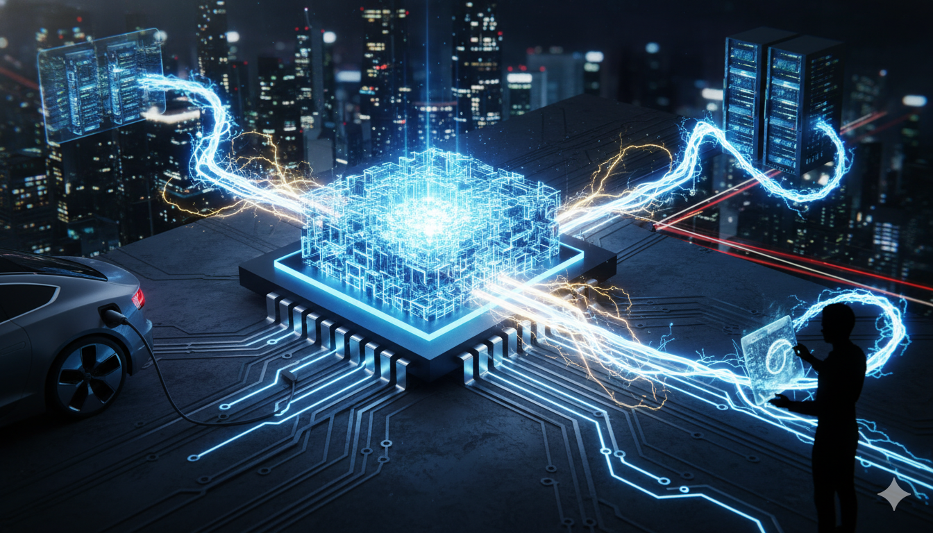
Powering the Invisible Transformation

Imagine plugging in your laptop and having it fully charged before your coffee cools—or adding 200 miles of range to your electric vehicle while grabbing lunch. These futuristic scenarios are no longer fantasy, thanks to gallium nitride (GaN), a powerful material at the heart of a silent energy revolution. While silicon has driven the information age for over half a century, GaN is rapidly becoming the go-to technology for the energy age—where efficiency, speed, and power density are paramount.

Unlike silicon, gallium nitride (GaN) offers a fundamentally superior foundation for modern power electronics, thanks to its wide bandgap, high thermal conductivity, and exceptional switching speed. These intrinsic material properties allow GaN devices to operate at higher voltages and frequencies while generating less heat—unlocking dramatic improvements in efficiency and performance. As a result, power systems built with GaN can be smaller, lighter, and significantly more energy-efficient than their silicon-based counterparts.

The practical benefits are already reshaping entire industries. A GaN-based charger, for example, can deliver three times the power output in half the size, eliminating the need for bulky power bricks. In electric vehicles, GaN inverters not only cut weight and system complexity but also extend driving range by up to 7%—a critical gain in a field where every watt counts. As our world accelerates toward electrification—across mobility, data, and the grid—GaN isn’t just a performance upgrade; it’s a transformational enabler of the next energy era.

Inside the Physics: Why GaN Outperforms Silicon

At the heart of GaN’s disruptive potential is its unique atomic structure, which grants it a bandgap of 3.4 electron volts (eV)—more than triple that of silicon’s 1.1 eV. This wider bandgap allows GaN devices to operate at much higher voltages, frequencies, and temperatures without performance degradation. In practical terms, GaN switches faster and more efficiently, reducing the energy lost as heat and enabling designs that are both more compact and more powerful.

In addition to its electrical advantages, GaN’s superior thermal conductivity minimizes heat buildup, significantly lowering the demand for bulky cooling solutions. This not only shrinks the physical footprint of power systems but also simplifies system design and lowers total cost of ownership. Together, these properties enable GaN to support the next generation of ultra-efficient, high-density power electronics—paving the way for lighter EV drivetrains, smaller chargers, more efficient solar inverters, and cooler-running data centers. GaN isn’t just a better switch—it’s the blueprint for power systems reimagined from the ground up.

2025: The GaN Tipping Point

This year marks a decisive turning point for GaN technology, with Infineon Technologies AG leading the charge through several landmark developments. Chief among them is the launch of GaN power semiconductor production on 300 mm wafers—a move that significantly boosts output while reducing cost per chip. According to Infineon, this transition enables 2.3 times more chips per wafer compared to the traditional 200 mm process, dramatically enhancing manufacturing efficiency and supply scalability. The larger wafer format also unlocks higher performance in terms of power density, thermal management, and system miniaturization—all while lowering overall system cost.

What makes this breakthrough even more impactful is that Infineon can leverage its existing high-volume 300 mm silicon manufacturing infrastructure, thanks to the compatibility between GaN and silicon processing. This strategic alignment not only accelerates time-to-market for advanced GaN components but also ensures efficient capital deployment. “Our existing production lines are ideal to pilot reliable GaN technology,” the company stated, emphasizing that this operational synergy strengthens supply chain resilience while enabling broad commercial deployment.

Infineon’s CEO, Jochen Hanebeck, framed the achievement as more than just a technical milestone. “This remarkable success is the result of our innovative strength and the dedicated work of our global team,” he noted. “It will be an industry game-changer and enable us to unlock the full potential of gallium nitride.” Coming just one year after Infineon’s acquisition of GaN Systems, this development reaffirms the company’s ambition to lead not only in GaN but across all key wide bandgap technologies—including silicon, silicon carbide (SiC), and gallium nitride (GaN).

To further cement its leadership, Infineon recently inaugurated a new semiconductor facility in Malaysia, dedicated to SiC converter production. Simultaneously, it has been ramping up R&D efforts in GaN technologies, with major pilot programs underway since May 2023. These strategic moves highlight Infineon’s long-term commitment to building a vertically integrated ecosystem for next-generation power electronics, combining material science leadership with manufacturing scale and innovation.

In parallel, Intel’s innovation with GaN-on-TRSOI (Trap-Rich Silicon-on-Insulator) substrates is pushing the boundaries of GaN’s performance envelope. By reducing leakage current by up to 50%, this breakthrough enhances both thermal stability and electrical efficiency, making it particularly well-suited for demanding AI accelerators and high-frequency telecom systems where energy density and heat dissipation are critical challenges.

At the same time, companies like EPC and Infineon are redefining what’s possible in power system architecture through monolithic integration. By embedding drivers, sensors, and protection circuits directly into GaN dies, these firms are eliminating traditional design bottlenecks such as parasitic inductance, which has historically limited switching performance. The result is a new class of compact, ultra-efficient devices capable of power densities exceeding 1 kW per cubic inch. Even more transformative is the introduction of bidirectional current flow, paving the way for next-generation vehicle-to-grid (V2G) systems, resilient energy storage, and high-efficiency DC/DC converters across transportation, industrial, and residential sectors.

Perhaps most significantly, GaN is beginning to push beyond its early 650V limits. Infineon’s 1,200V GaN prototype, now in customer testing, extends its reach into higher-voltage applications traditionally dominated by silicon carbide (SiC), particularly for DC/DC converters and auxiliary power systems in EVs and grid infrastructure.

GaN in Action: Transforming Mobility, AI, and the Grid

The real-world impact of GaN is already visible across multiple industries. In electric vehicles, GaN enables ultra-compact on-board chargers (OBCs) that are 30% lighter yet capable of delivering over 20 kW—nearly triple what silicon-based chargers manage. In hybrid vehicles, 48V to 12V DC/DC converters built with GaN have achieved remarkable efficiencies of up to 99.3%, making every watt count in power-constrained designs.

In data centers powering the AI boom, the demand for higher power densities has made GaN indispensable. Where once 3.3 kW per server rack sufficed, today’s AI workloads demand upwards of 12 kW per rack, forcing engineers to turn to GaN-based power stages for their superior efficiency and thermal performance. Some designs even combine GaN and SiC technologies in hybrid modules, optimizing both voltage handling and switching speed to meet these extreme requirements.

Renewable energy systems are also benefiting from GaN’s capabilities. In solar inverters, GaN has pushed conversion efficiencies beyond 99%, significantly shortening payback periods for both residential and commercial installations. When paired with home energy storage systems, GaN not only improves efficiency but also reduces size and cost—accelerating the transition to solar-plus-storage models in smart homes worldwide.

Riding the Market Surge: GaN by the Numbers

The GaN market is entering a phase of rapid acceleration. In 2024, the global GaN semiconductor market is estimated at $1.42 billion. By 2030, it’s projected to reach $3.43 billion, fueled by a compound annual growth rate of 19.1%. More specifically, GaN power device sales are expected to jump from $288 million to $4.04 billion, marking a staggering 34.1% CAGR. In the EV sector, GaN’s role is pivotal—enabling the leap from 14% to over 30% global EV adoption by 2030. In parallel, power demands in data centers are expected to triple, making GaN a critical enabler of the AI revolution.

GaN vs. SiC: Friends, Not Foes

At the 2025 Applied Power Electronics Conference (APEC), industry leaders reached a clear consensus: gallium nitride (GaN) and silicon carbide (SiC) are not rivals but complementary tools in the next-generation power electronics toolbox. GaN thrives in sub-900V applications where speed, efficiency, and integration matter most—think fast chargers, RF amplifiers, and ultra-compact data center power supplies. Its high switching frequency and low parasitic losses make it the material of choice for compact, high-efficiency designs.

Meanwhile, SiC’s ruggedness under high voltage and high temperature gives it a decisive edge in harsh, high-power applications, such as traction inverters for electric vehicles, industrial drives, and utility-scale grid converters. Its thermal stability and high breakdown voltage allow it to operate reliably where GaN would struggle. As Microchip’s Kevin Speer aptly summarized, “Don’t force GaN into traction inverters or SiC into phone chargers.” Each material excels in its own domain, and together, they are enabling a layered, optimized approach to electrification across industries.

Overcoming the Last Hurdles

Despite its immense promise, gallium nitride (GaN) still faces a few critical challenges before it can achieve mainstream ubiquity. Reliability remains a top concern, especially in mission-critical applications like automotive and aerospace. Traditional qualification methods such as H3TRB (High Temperature, High Humidity, High Voltage Reverse Bias) are no longer sufficient on their own. To address this, manufacturers are now implementing mission-specific stress tests that simulate real-world operating conditions—ensuring GaN devices can withstand the thermal, electrical, and mechanical demands of their intended environments.

Packaging is another bottleneck. Legacy packages like TO-247, originally designed for slower-switching silicon devices, simply can’t support the ultra-fast switching speeds and high frequencies at which GaN excels. These outdated formats introduce parasitic inductance that limits performance and creates thermal challenges. In response, the industry is rapidly shifting toward embedded module solutions and chip-scale packaging (CSP), which offer lower inductance, better thermal management, and tighter integration. Overcoming these final engineering barriers is essential to unlock GaN’s full potential across consumer, industrial, and transportation sectors.

On the geopolitical front, China is emerging as a major force, having invested over $41 billion into its GaN and SiC industries. The country aims to control up to 40% of the global wide bandgap semiconductor market by 2030, raising strategic questions about supply chains and innovation leadership.

Tomorrow’s GaN: Beyond 2025

The future of GaN is not just promising—it’s accelerating. As research and commercialization efforts mature, new frontiers are opening across robotics, communications, and high-voltage infrastructure. In robotics, GaN is powering the next wave of ultra-compact motor drivers for humanoid robots, autonomous drones, and agile delivery platforms. Thanks to its thermal efficiency and high-frequency switching, these systems eliminate the need for bulky heatsinks, enabling more compact, lightweight, and energy-efficient designs.

In the realm of wireless communication, GaN’s high electron mobility and frequency performance are becoming indispensable for building terahertz-frequency amplifiers, a critical component of 6G networks. These amplifiers will drive faster data transmission and more efficient spectrum use, enabling future innovations in real-time connectivity, immersive media, and intelligent edge devices.

Perhaps most significantly, vertical GaN architectures are beginning to reshape GaN’s role in high-voltage applications. Companies like NexGen are pioneering designs that push breakdown voltages beyond 2,000 volts, putting GaN into direct competition with SiC in domains once considered out of reach—such as industrial motor drives, utility-scale solar inverters, and traction inverters for EVs. As these technologies converge, GaN is evolving from a niche high-efficiency solution into a foundational platform for next-generation power electronics.

Conclusion: The Silent Efficiency Revolution

Gallium nitride is more than a breakthrough in semiconductor physics—it’s a cornerstone of the global energy transformation. By eliminating inefficiencies across the power chain—from mobile devices to EVs, from data centers to solar arrays—GaN is quietly but powerfully driving a more sustainable, electrified future. Industry leaders predict that GaN adoption could reduce global carbon emissions by over 100 megatons of CO₂ annually by 2030. As Infineon’s Johannes Schoiswohl puts it, “GaN’s tipping point isn’t coming—it’s here.” And with it comes the promise of a world where power is faster, smaller, cooler—and infinitely smarter.


▶️ Dive Deeper

About Rajesh Uppal

Check Also

Unleashing Geothermal Power: The Clean Energy Revolution Accelerated by Breakthrough Technologies

Introduction: The Sleeping Giant Awakens Geothermal energy, long considered a niche renewable, is experiencing a …

wpChatIcon
wpChatIcon