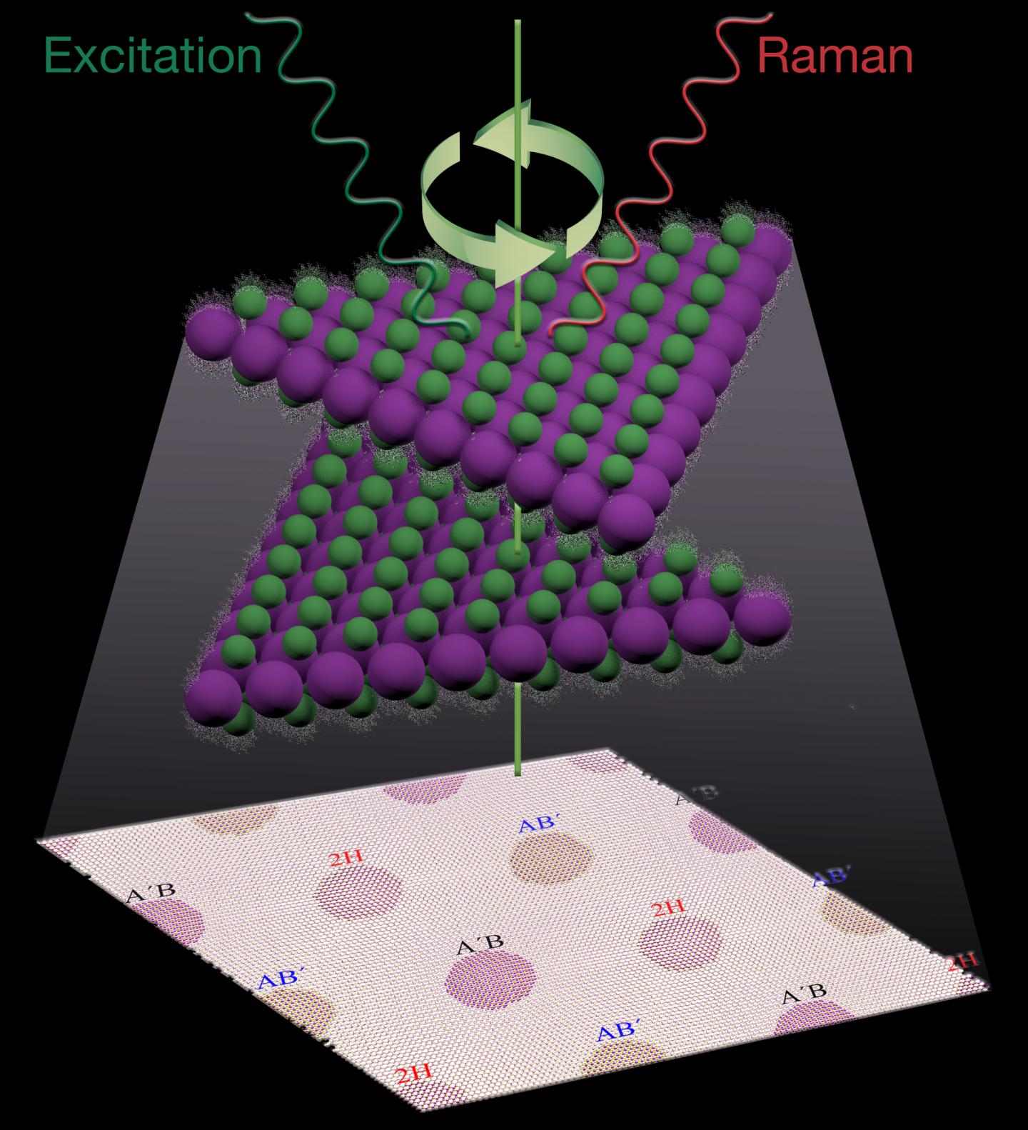
When two atomically thin two-dimensional layers are stacked on top of each other and one layer is made to rotate against the second layer, they begin to produce patterns — the familiar moiré patterns — that neither layer can generate on its own and that facilitate the passage of light and electrons, allowing for materials that exhibit unusual phenomena. For example, when two graphene layers are overlaid and the angle between them is 1.1 degrees, the material becomes a superconductor.
“It’s a bit like driving past a vineyard and looking out the window at the vineyard rows. Every now and then, you see no rows because you’re looking directly along a row,” says Nathaniel Gabor, an associate professor in the Department of Physics and Astronomy at the University of California, Riverside.
“This is akin to what happens when two atomic layers are stacked on top of each other. At certain angles of twist, everything is energetically allowed. It adds up just right to allow for interesting possibilities of energy transfer.”
Stacking layers of nanometer-thin semiconducting materials at different angles offers a new approach for designing the next generation of energy-efficient transistors and solar cells. The atoms in each layer are arranged in hexagonal arrays; when two layers are stacked and rotated, atoms in one layer overlap with those in the other layer and can form an infinite number of overlapping patterns. This is like the Moiré patterns that result when two screens are overlaid and one is rotated on top of the other.
To bring it all under one roof, Nathaniel Gabor of University of California, Riverside and physicist Justin C. W. Song of Nanyang Technological University, Singapore, have proposed this field of research be called “electron quantum metamaterials” and have just published a perspective article in Nature Nanotechnology. “We highlight the potential of engineering synthetic periodic arrays with feature sizes below the wavelength of an electron. Such engineering allows the electrons to be manipulated in unusual ways, resulting in a new range of synthetic quantum metamaterials with unconventional responses,” Gabor says.
Metamaterials are a class of material engineered to produce properties that do not occur naturally. Examples include optical cloaking devices and super-lenses akin to the Fresnel lens that lighthouses use. Nature, too, has adopted such techniques — for example, in the unique coloring of butterfly wings — to manipulate photons as they move through nanoscale structures. “Unlike photons that scarcely interact with each other, however, electrons in subwavelength structured metamaterials are charged, and they strongly interact,” Gabor says. “The result is an enormous variety of emergent phenomena and radically new classes of interacting quantum metamaterials.”