Modern warfare is increasingly dependent on microelectronics capabilities that sense the environment, convert the signals into data streams, process the information, and generate a response. In this sense, Aerospace and Defense (A-D) systems are quite similar to commercial systems that perform communications and computations, while taking advantage of the advancement of semiconductor density, functionality, and cost reduction due to Moore’s Law. There is the everincreased demand for more data throughput through wired and wireless systems. Cellular systems have migrated from 3G to 4G and now 5G architectures which improves bandwidth ~10X with each generation. DoD systems for communications, radar, and sensing generally require wider bandwidths, higher dynamic range, and higher transmit power, as well as specialized frequency bands and security requirements that the commercial side does not require.
Several characteristics of the A-D sector create unique challenges, They are high performance so require access to leading silicon nodes and advanced packaging technologies to maintain advantage in specific technical metrics (e.g., digitization over wide bandwidths and at high dynamic range. They require High Reliability as they need to survive in harsh environments, prioritize human safety in high-risk environment. They require Long Product Lifecycles therefore managing parts obsolescence and upgradability is important. Compared to commercial sector they are Low Volumes hence require access to supply chain that provides high product mix, and business models where
NRE is managed without high volumes for amortization. finally Security is paramount and hence require secure domestic supply chain and/or verification technologies.
Heterogeneous integration is a factor in all of these challenges, whether by adding new twists to the challenges with multiple device technologies or by solving some of them with modular designs and assemblies. Most specifically, heterogeneous integration directly addresses the high-performance challenge for the A-D sector.
Heterogeneous integration via 2.5D technology is approaching mainstream status, with industry leaders such as Xilinx, Intel, Nvidia, and AMD using it in their leading products. They have identified the benefits of splitting up silicon functionality, whether to improve yield with smaller chips, as Xilinx did with their pioneering FPGA “slices,” or to enable the integration of different types of devices.
Monolithic System on a Chip solutions are becoming increasingly limited for A-D applications. Sustaining Moore’s Law by increasing the core count on a die is not feasible as memory access bottlenecks prevail and die size and complexity become prohibitively expensive. Diversity in process nodes and materials are needed (CPUs, GPUs, FPGAs) for enhancing performance, energy efficiency and programmability. Similarly, RF/mm-wave devices and data converters are needed for communications and sensing. Heterogeneous integration offers a way to address these limitations and sustain Moore’s Law through interconnect length reductions and optimal combinations of different device technologies. The A-D sector must adapt and adopt innovation and market drivers from the commercial semiconductor industry.
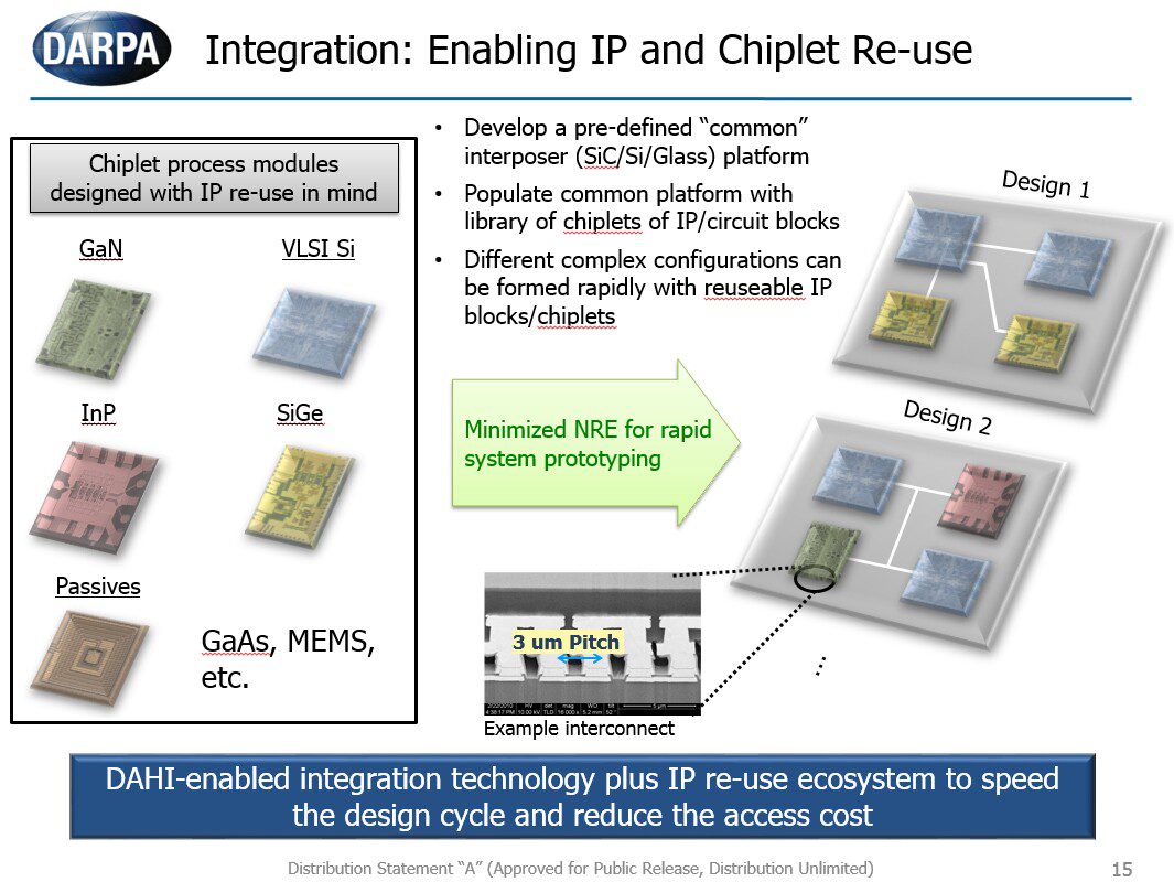
DARPA has led the way in advancing Heterogeneous Integration Technology through a number of programs. The DARPA DAHI program demonstrated the feasibility of 2.5D HI for integration of CMOS devices with high-performance III-V devices through both die-to-wafer and wafer-to-wafer bonding techniques. The DARPA CHIPS program (which is still on-going) is developing a 2.5D chiplet ecosystem and a set of standard interfaces for chiplet to chiplet communications.
By enabling this heterogeneous integration capability, DAHI seeks to establish a new paradigm for microsystems designers to utilize a diverse array of materials and device technologies on a common silicon-based platform. DARPA launched Common Heterogeneous Integration and Intellectual Property (IP) Reuse Strategies (CHIPS) program seeking innovative insights on how standard interfaces and IP reuse can be to create custom circuits in a fraction of today’s time and cost, with conventional methods for both digital and analog systems.
On June 1, 2017, the DARPA Microsystems Technology Office (MTO) announced a new Electronics Resurgence Initiative (ERI) to ensure far-reaching improvements in electronics performance well beyond the limits of traditional scaling. The ERI will draw on new and existing DARPA programs to make a significant investment into enabling circuit specialization and managing complexity. The foundation for the Initiative has been building for a number of years in the form of existing MTO programs such as DAHI, CHIPS and CRAFT, which address ERI’s three research pillars: materials and integration, circuit design, and systems architecture.
These DARPA Programs are in line with US’s third offset strategy, which according to Hagel is “This new initiative is an ambitious department-wide effort to identify and invest in innovative ways to sustain and advance America’s military dominance for the 21st century.” Instead of such custom-tailored, tightly integrated systems, you want a modular and open architecture where you can easily replace a component — hardware or software — without disrupting the rest of the system. Instead of a relatively small number of pricey manned platforms, you want a “heterogeneous” mix of manned and unmanned vehicles of all kinds, from 130-foot robotic ships to disposable handheld drones. Instead of architectures designed for a specific kind and size of force, you want systems that can scale up and down as the force changes.