The emerging field of printed electronics requires a suite of functional materials for applications including flexible and large-area displays, radio frequency identification tags, portable energy harvesting and storage, biomedical and environmental sensor arrays, and logic circuits.
To enable these technologies, functional materials must be integrated with suitable patterning technologies, such as inkjet, gravure, and flexographic printing. Because electrical conductors are a core component of electronic devices, significant effort has been devoted to conductive materials in the field of printable inks. Common conductive inks can be classified into three categories: noble metals, conductive polymers, and carbon nanomaterials.
Graphene is a 1-atom-thick layer of tightly bonded carbon atoms arranged in a hexagonal lattice. Graphene the world’s first 2D nanomaterial, is widely regarded as the “wonder material” of the 21st century due to the combination of its extraordinary properties. As a single layer of graphite, it is the thinnest material (monoatom thick), transparent, 200 times stronger than steel, yet as flexible as rubber, more conductive than copper, excellent thermal conductor and impermeable to moisture and gases. Graphene is also extraordinarily light at 0.77 mg/m2, which is roughly 1,000 times lighter than 1 m2 of paper. It is fire resistant yet retains heat.
Wearable electronic textiles (e-textiles) have become a focus of significant research interest due to their potential applications in sportswear, military uniforms, environmental monitoring and health care. There have been enormous efforts in incorporating electronic components to make e-textiles for various applications such as sensors, energy storage devices, transistors and photovoltaic devices.
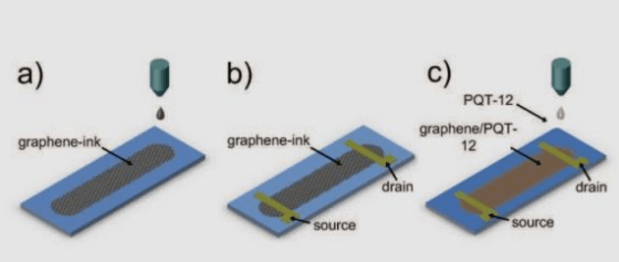
Researchers are exploring the potential of graphene for the fabrication of the next generation e-textiles. Inkjet printing of graphene inks is considered to be very promising for wearable e-textile applications as benefits of both inkjet printing and extra-ordinary electronic, optical and mechanical properties of graphene can be exploited.
Vorbeck came out with their Vor-Ink series, and for the first time one could order a bucket of conductive graphene paint online. Vorbeck also patented graphene for use in conductive inks. The Cambridge Graphene center has partnered with Plastic Logic a leader in organic transistors and plastic electronics. One of the key research directions in this collaboration is printed electronics.
In September 2013, Graphene Platform and Japan’s Nissha Printing partnered to deliver products based on graphene inks developed at University of Cambridge.
In November 2013, IDTechEx recognized the potential of graphene for printed electronics and awarded Durham Graphene Science (DGS) its Best Technical Development Materials Award. DGS is a spinout company of Durham University. The company “won this award for its high specification graphene production process that can seem to scale to large-volume, utilizing a bottom-up synthesis method. DGS, has recently completed the commissioning of its first commercial scale facility, which is capable of producing one tonne of high-purity graphene nanoplatelets per year”.