Optical atomic clocks are at the pinnacle of time measuring devices, losing less than one second every ten billion years. Currently though, they are massive devices, weighing hundreds of kilograms. In order to have an optimal practical function that could be utilised by your average person, their size needs to be greatly reduced whilst retaining the accuracy and speed of the large-scale clocks.
Dr. Alessia Pasquazi from the EPic Lab in the School of Mathematical and Physical Sciences at the University of Sussex explains the breakthrough: “With a portable atomic clock, an ambulance, for example, will be able to still access their mapping whilst in a tunnel, and a commuter will be able to plan their route whilst on the underground or without mobile phone signal in the countryside. Portable atomic clocks would work on an extremely accurate form of geo-mapping, enabling access to your location and planned route without the need for satellite signal.
Militaries are also interested in technologies in GPS denied environments. GPS is vulnerable to jamming attacks, GNSS jammers are now being used by criminals or vehicle hijackers, as reported by the FBI: “GPS tracking devices have been jammed by criminals engaged in nefarious activity including cargo theft and illicit shipping of goods.Typical military jammers are able to affect GPS receiver for many tens of kilometers by line of sight. It’s a problem because best accuracy, availability and global coverage of PNT data is through GPS/GNSS.
One of the approach militaries are developing is integration of GPS with complementary technologies such as chip-scale atomic clocks and small inertial measurement units of the Microelectromechanical Systems (MEMS).
Scientists in the Emergent Photonics Lab (EPic Lab) at the University of Sussex have made a breakthrough to a crucial element of an atomic clock—devices which could reduce our reliance on satellite mapping in the future—using cutting-edge laser beam technology. Their development greatly improves the efficiency of the lancet (which in a traditional clock is responsible for counting), by 80% – something which scientists around the world have been racing to achieve.
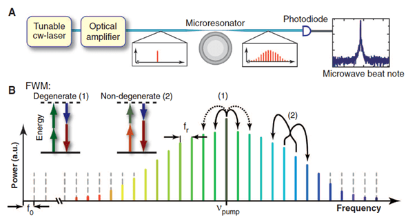
Optical frequency combs serve as the clockwork of optical clocks, which are now the best time-keeping systems in existence. In optics, a frequency comb is a laser source whose spectrum consists of a series of discrete, equally spaced frequency lines. Frequency combs can be seen as many single frequency, continous-wave lasers whose emission frequencies are different but equidistant and whose emission is coherent between all the lasers.
Frequency combs can be generated by a number of mechanisms, including periodic modulation (in amplitude and/or phase) of a continuous-wave laser, four-wave mixing in nonlinear media, or stabilization of the pulse train generated by a mode-locked laser. Conventionally frequency combs generated using pulsed, mode locked lasers – the time frequency duality implies that an ultra-short pulse laser will create an optical comb in the frequency domain. In one of the schemes , a single laser is coupled into a microresonator (such as a microscopic glass disk that has whispering-gallery modes). This kind of structure naturally has a series of resonant modes with approximately equally spaced frequencies.
A major challenge has been how to make such comb sources smaller and more robust and portable. In the past 10 years, major advances have been made in the use of monolithic, chip-based microresonators to produce such combs. While the microresonators generating the frequency combs are tiny—smaller than a human hair—they have always relied on external lasers that are often much larger, expensive, and power-hungry.
Researchers at Columbia Engineering announced in Nature in Oct 2018, that they have built a Kerr frequency comb generator that, for the first time, integrates the laser together with the microresonator, significantly shrinking the system’s size and power requirements. They designed the laser so that half of the laser cavity is based on a semiconductor waveguide section with high optical gain, while the other half is based on waveguides, made of silicon nitride, a very low-loss material. Their results showed that they no longer need to connect separate devices in the lab using fiber—they can now integrate it all on photonic chips that are compact and energy efficient.