Home / Technology / Electronics & EW / Transparent Electronics enabled by new materials promise invisible electronic circuitry and opto-electronic devices and radar-absorbing coatings on fighter planes

Transparent Electronics enabled by new materials promise invisible electronic circuitry and opto-electronic devices and radar-absorbing coatings on fighter planes

Transparent electronics is an emerging science and technology field focused on producing invisible electronic circuitry and opto-electronic devices. The transparent electronic devices and transparent electronic circuits have wide range of applications. Transparent Conducting Oxides (TCOs) and Thin Film Transistors (TFTs) are used in the production of transparent electronics.


The progressions in transparent electronics technology are mainly dependent on advancements in manufacturing processes and material sciences. Transparent electronics offer various advantages over conventional electronics, such as lower processing temperature; strong performance, mobility and flexibility; high voltage gain; heat dissipation; and radiation tolerances. Owing to these characteristics, they are being utilized in consumer electronic products and new energy sources such as next-generation televisions, mobiles, computers and solar panels.


Apart from this, technological innovations have presented new application areas of transparent electronics including transparent solar cells, navigation display for military equipment and OLED displays. Circuits built from ultrathin, single crystal silicon are also being used in the medical field


Almost every glass setting can be modified in to electronic device; windows could also be used as power generator, automobile windshields could transmit visual information to the driver, consumer electronics, security systems, in military for real-time wearable displays.


In consumer electronics LCD displays, iPad and smart-phone touch screens, and organic light-emitting diode (OLED) displays for televisions and computer monitors could be fabricated by using transparent electronic devices. Transparent electronics is also useful for military applications. Using navigation display soldiers can see real-time video and graphics information. It must be full colored and of high information content. This can be provided using organic light-emitting devices (OLEDs).


Transparent technologies

There have been significant advancements in the materials and designs of transparent electronics along with the introduction of innovative processing methods. For instance, the development of new ceramic thin films containing multi-component oxides has enabled the manufacturers to use them in both rigid and flexible transparent electronics.


However, the device building block materials, the semiconductor, the electric contacts, and the dielectric/passivation layers, must now be transparent in the visible a true challenge. Therefore, the first scientific goal of this technology must be to discover, understand, and implement transparent high-performance electronic materials. The second goal is their implementation and evaluation in transistor and circuit structures. The technology of transparent electronics is extremely costly to manufacture. That means, by the time it is mass produced, the costs will add up even more.


You have a heads up display in your car because of the simple fact that it is an expensive one. It is a technology that is found only in some of the high-end luxury cars. That means, it isn’t a cheap technology. It isn’t cheap because of the very principles of Physics that it has follow. The amalgamation of the opto and electro capabilities of a device is extremely hard to achieve. The challenge is that the transistor materials must be transparent to visible light yet have good carrier mobility. This requires a special class of materials having contra-indicated properties because from the band structure point of view, the combination of transparency and conductivity is contradictory.


Transparent semiconductors such as GaN and diamond are already known, but they come at high cost which makes them impossible to use in transparent electronic devices demanding relatively large screens, such as displays. The two technologies which preceded and underlie transparent electronics are Transparent Conductive Oxides(TCOs) and Thin- Film Transistors (TFTs).


Transparent Conductive Oxides(TCOs)

TCOs constitute an unusual class of materials possessing two physical properties- high optical transparency and high electrical conductivity. They are generally considered to be mutually exclusive. This peculiar combination of physical properties is only achievable if a material has a sufficiently large energy band gap so that it is non-absorbing or transparent or transparent to visible light, and also possesses a high enough concentration with a sufficiently large mobility that the material can be considered to be a good conductor of electricity. The three most common TCOs are indium oxide, tin oxide, and zinc oxide. All these materials have band gaps above that required for transparency across the full visible spectrum. Graphene is transparent and can be used as a potential material.


Transparent Thin Film Transistors (TTFTs)

Thin-Film Transistors are another technology underlying transparent electronics, since it is a bridge between passive electrical and active electronic applications. Transparent Thin Film Transistors are made by depositing thin films of semiconductor active layer as well as the dielectric layer and a metallic contact over a supporting subtract. The challenge for producing Transparent electronics and opto electronic circuits is that the transistor should promote high performance with minimal fabrication. It should also have a good mobility and the potential for the device to function.


Transparent UV detector

Transparent UV detector contain a pn-junction of a wide band gap semiconductor. It is helpful for detecting UV radiation intensity. A transparent UV-detector was fabricated by using a high quality pn-heterojunction diode composed of ptype NiO: Li and n-type ZnO and its UV response measured at room temperature.


Silver nanowires as transparent electronic material

A submicrometer-thin mesh of silver nanowires—that is transparent to light, highly electrically conductive, flexible and stretchable, and simple to make—has been developed by researchers at KAUST. The material could find use in flexible electronic displays, sensors, solar cells or even incubators for newborn babies.


There are printed films of metal nanowires in which the conductive metal nanowires are so thin that light can pass between them. However, it has been challenging to directly create nanowire sheets that simultaneously have high conductivity, high transparency, flexibility and stretchability. “Now, we have found a solution to this problem,” explains Weiwei Li, a postdoctoral researcher in Shamim’s team.


First, the team refined the method for making silver nanowires, adapting the previous protocol to make larger quantities of longer nanowires. The nanowires could be used directly in a new ink formulation that resulted in a uniform layer of silver when applied by screen printing onto a flexible substrate.


Thanks to the length of the nanowires, the team could achieve high conductivity with a relatively sparse covering of nanowires, that in turn improved optical transparency. In a final manufacturing step, the team used laser sintering to weld together adjacent nanowires at points of contact: this improved electrical conductivity further while also reducing the thickness of the silver layer and letting even more light pass through. The material maintained its electrical performance even after 1000 stretch-release cycles and 1000 bending cycles.


The team tested their material’s performance by printing the conductive ink in patterns that enabled it to absorb predetermined wavelengths of electromagnetic radiation. “With the huge number of wireless devices, we are all exposed to electromagnetic radiation all the time,” Li says. “We designed special electromagnetic absorbers using our transparent ink which can absorb more than 90 percent of the electromagnetic signals in a specific frequency band,” he explains.


“We believe that this work will benefit the development of future flexible, transparent and stretchable conductive electronics at low cost and at large scale,” says Shamim. Other potential applications include radar-absorbing coatings to cover the curved surface of fighter planes, rendering them invisible to enemy radar systems.


Nylon as a building block for transparent electronic devices

Scientists have solved a four decade long challenge of producing very thin nylon films that can be used for instance in electronic memory components. The thin nylon films are several 100 times thinner than human hair and could thus be attractive for applications in bendable electronic devices or for electronics in clothing.


Nylons, a family of synthetic polymers, were first introduced in the 1940s for women’s stockings and are nowadays among the most widely used synthetic fibers in textiles. They consist of a long chain of repeated molecular units, i.e. polymers, where each repeat unit contains a specific arrangement of hydrogen, oxygen, and nitrogen with carbon atoms.


Besides the use in textiles, it was discovered that some nylons also exhibit so called “ferroelectric properties.” This means that positive and negative electric charges can be separated and this state can be maintained. The ferroelectric materials are used in sensors, actuators, memories and energy harvesting devices. The advantage in using polymers is that they can be liquified using adequate solvents and therefore processed from solution at low cost to form flexible thin-films which are suitable for electronic devices such as capacitors, transistors and diodes. This makes ferroelectric polymers a viable choice for integration with e-textiles. Although nylon polymers have found over the years significant commercial applications in fabrics and fibers, their application in electronic devices was hindered because it was impossible to create high quality thin films of ferroelectric nylons by solution processing.


Scientists at the MPI-P, in collaboration with researchers from the Johannes Gutenberg University of Mainz and Lodz University of Technology, have now solved this forty year old problem, and developed a method to fabricate ferroelectric nylon thin-film capacitors by dissolving nylon in a mixture of trifluoroacetic acid and acetone and solidifying it again in vacuum. They were able to realize thin nylon films that are typically only a few 100 nanometers thick, several 100 times thinner than human hair. “Using this method, we have produced extremely smooth thin-films. This is very important because it prevents electrical break down of for example capacitors and destroying the electronic circuits. At the same time, the smoothness allows for having transparent thin-films and eventually transparent electronic devices,” says Dr. Kamal Asadi, group leader at the MPI-P.


By using their newly developed method, the group around Kamal Asadi was able to produce high performance nylon capacitors. The scientists subjected the prototypes of the capacitors to extended stress cycles and demonstrated robustness of ferroelectric nylons under millions of operation cycles. The thin nylon films could become an important component for use in flexible electronics in the future and find applications in bendable electronic devices or for electronics in clothing. These new findings pave the way towards multi-functional fabrics that serve as cloth for covering our body and at the same time can generate electricity from our body movement.


Transparent Electronics Market

The Transparent Electronics Market was valued at USD 996.25 million in 2019 and is expected to reach USD 3800.39 million by 2025, at a CAGR of 25% over the forecast period 2020 – 2025.


Growing penetration of touch-enabled electronic devices is driving the market as it can be seen as a substitution for the traditional keypad/keyboard and mouse. This multi-touch technology is in great demand with multi-touch enabled products such as smartphones & tablets, and they have a big share in the market in the future. Consumer electronic products are the ones that contribute maximum to these devices.


In the last decade, the market for different materials used in transparent electronic applications has grown robustly. This emerging market is expected to grow at a speculative rate in the future. Due to many tech savvy people, a majority of this growth is expected from North America and Europe.


Silicon compounds are expected to have a major impact and can become a driving factor for the transparent electronic materials market. Oxide semiconductors are liable to be transparent which means one can build transparent circuits and this allows to build transparent displays. The application of transparent circuits could be smart windows that change transparency upon changes in the environment (heat, light, voltage).


The silicon compound segment is dominating the transparent electronic materials market. Zinc oxide is the cheapest and an environment friendly compound; it also has significant potential in non-volatile flash memory.

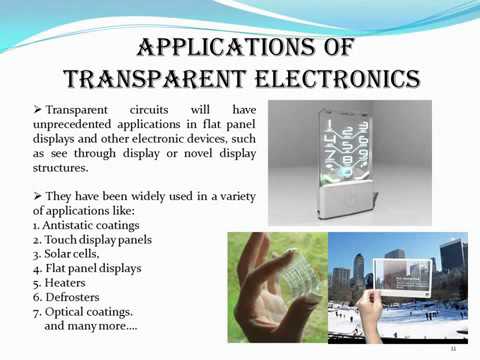
The market was dominated by transparent conducting oxides (TCO) due to their wide range of applications in touch display panels, optical coatings, flat panel displays, solar cells, defrosters, heaters, optical coating, and smart windows. TCOs can be used as passive optical or electrical coatings. The silicon compound segment is dominating the transparent electronic materials market. Zinc oxide is the cheapest and an environment friendly compound; it also has significant potential in non-volatile flash memory.


Transparent electronics reduce the size and increase the memory capacity of electronic devices. Moreover, market growth is further accelerated by technology innovation and new product developments, which will reduce the cost and size of electronic devices.


The Oregon State University has developed zinc tin oxide based resistive random access memory (RRAM) which is also referred to as ‘memristor’. This is a new transparent technology which the computer memory operates on resistance. Products incorporated with this technology become cheaper, smaller, and faster.


Experts say that while the market for transparent electronics will surely grow in the next two or three decades, there are several things that need to be addressed for it to happen. Manufacturers have to keep in mind of the aesthetics of the products. Apart from being functional, any product should be easy to use and at the same time should have a visual appeal.


Top Companies in Global Transparent Electronics Market include BOE Technology Group Co., Brite Solar Inc., ClearLED Ltd., Corning Incorporated, LG Electronics Inc., Shenzhen AuroLED Technology Co.,Ltd, Shenzhen Nexnovo Technology Co., Ltd, Street Communication Inc., Ubiquitous Energy Inc., Panasonic Corporation


References and Resources also include:

http://www.ijircce.com/upload/2017/april/202_A%20Study.pdf

https://www.military-technologies.net/2018/04/13/transparent-electronics-market-technology-innovation-and-new-product-developments/

https://www.sciencedaily.com/releases/2019/08/190816191445.htm

https://phys.org/news/2019-10-baby-transparent-electronics.html

About Rajesh Uppal

Check Also

DARPA’s Rubble to Rockets (R2) Program: Revolutionizing Forward Production with Indigenous Materials

In an age where the battlefield is as much about innovation as it is about …

error: Content is protected !!